SN74AVC4T245

Features: Control Inputs VIH/VIL Levels are Referenced to VCCA VoltageFully Configurable Dual-Rail Design Allows Each Port to Operate Over the Full 1.2-V to 3.6-V Power-Supply RangeI/Os Are 4.6-V TolerantIoff Supports Partial-Power-Down Mode OperationPinoutSpecificationsSupply voltage range, VCCA ...

product image

SN74AVC4T245 Picture
SeekIC No. : 004498554 Detail

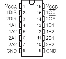
SN74AVC4T245: Features: Control Inputs VIH/VIL Levels are Referenced to VCCA VoltageFully Configurable Dual-Rail Design Allows Each Port to Operate Over the Full 1.2-V to 3.6-V Power-Supply RangeI/Os Are 4.6-V To...

floor Price/Ceiling Price

Part Number:
SN74AVC4T245
Supply Ability:
5000

Price Break

  • Qty
  • 1~5000
  • Unit Price
  • Negotiable
  • Processing time
  • 15 Days
Total Cost: $ 0.00

SeekIC Buyer Protection PLUS - newly updated for 2013!

  • Escrow Protection.
  • Guaranteed refunds.
  • Secure payments.
  • Learn more >>

Month Sales

268 Transactions

Rating

evaluate  (4.8 stars)

Upload time: 2025/12/24

Payment Methods

All payment methods are secure and covered by SeekIC Buyer Protection PLUS.

Notice: When you place an order, your payment is made to SeekIC and not to your seller. SeekIC only pays the seller after confirming you have received your order. We will also never share your payment details with your seller.
Product Details

Description


Features:

 Control Inputs VIH/VIL Levels are Referenced to VCCA Voltage
 Fully Configurable Dual-Rail Design Allows Each Port to Operate Over the Full 1.2-V to 3.6-V Power-Supply Range
 I/Os Are 4.6-V Tolerant
 Ioff Supports Partial-Power-Down Mode Operation


Pinout

  Connection Diagram


Specifications

Supply voltage range, VCCA and VCCB  . . . . . . . . . . . . . . . . . . . . . . . . . . . . . . . . .  . . . . .−0.5 V to 4.6 V
Input voltage range, VI (see Note 1): I/O ports (A port)  . . . . . . . . . . . . . . . . .  . . . . . . .−0.5 V to 4.6 V
                                                            I/O ports (B port)  . . . . . . . . . . . . . .  . . . . . . . . . .−0.5 V to 4.6 V
                                                            Control inputs  . . . . . . . . . . . . . . . . . . . . . . . . . . .−0.5 V to 4.6 V
Voltage range applied to any output in the high-impedance or power-off state, VO
     (see Note 1): (A port)  . . . . . . . . . . . . . . . . . . . . . . . . . . . . . . . . . . . . . . . . . . . . . . . . .−0.5 V to 4.6 V
                           (B port)  . . . . . . . . . . . . . . . . . . . . . . . . . . . . . . . . . . . . . . . . . . . . . . . . .−0.5 V to 4.6 V
Voltage range applied to any output in the high or low state, VO
     (see Notes 1 and 2): (A port)  . . . . . . . . . . . . . . . . . . . . . . . . . . . . . . . . . . . . .−0.5 V to VCCA + 0.5 V
                                       (B port) . . . . . . . . . . . . . . . . . . . . . . . . . . . . . . . .  . . . . .−0.5 V to VCCB + 0.5 V
Input clamp current, IIK (VI < 0)  . . . . . . . . . . . . . . . . . . . . . . . . . . . . . . . . . . . . .. . . . . . . . . . . . .−50 mA
Output clamp current, IOK (VO < 0)  . . . . . . . . . . . . . . . . . . . . . . . . . . . . . . . . . . . . .. . . . . . . . . . .−50 mA
Continuous output current, IO  . . . . . . . . . . . . . . . . . . . . . . . . . . . . . . . . . . . . . . . . . . . . . . . . . . .±50 mA
Continuous current through VCCA, VCCB, or GND . . . . . . . . . . . . . . . . . . . . . . .  . . . . . . . . . . . . .±100 mA
Package thermal impedance, JA (see Note 3): D package  . . . . . . . . . . . . . .. . . . . . . . . . . . . . . .73°C/W
                                                    (see Note 3): DB package  . . . . . . . . . . . . .  . . . . . . . . . . . . . . .82°C/W
                                                    (see Note 3): DGV package  . . . . . . . . . . . .. . . . . . . . . . . . . . .120°C/W
                                                    (see Note 3): PW package  . . . . . . . . . . . . .  . . . . . . . . . . . . . .108°C/W
                                                    (see Note 4): RGY package  . . . . . . . . . . . . . . . . . . . . . . . . . . . .39°C/W
Storage temperature range, Tstg  . . . . . . . . . . . . . . . . . . . . . . . . . . . . . . . . . . . . . . . . . . .−65°C to 150°C


Description

This SN74AVC4T245 4-bit noninverting bus transceiver uses two separate configurable power-supply rails. The A port is designed to track VCCA. VCCA accepts any supply voltage from 1.2 V to 3.6 V. The B port is designed to track VCCB. VCCB accepts any supply voltage from 1.2 V to 3.6 V. This allows for universal low-voltage bidirectional translation between any of the 1.2-V, 1.5-V, 1.8-V, 2.5-V, and 3.3-V voltage nodes.

The SN74AVC4T245 is designed for asynchronous communication between data buses. The device transmits data from the A bus to the B bus or from the B bus to the A bus, depending on the logic level at the direction-control (DIR) input. The output-enable (OE) input can be used to disable the outputs so the buses are effectively isolated.

The SN74AVC4T245 is designed so that the control pins (1DIR, 2DIR, 1OE, and 2OE) are supplied by VCCA.

This SN74AVC4T245 device is fully specified for partial-power-down applications using Ioff. The Ioff circuitry disables the outputs, preventing damaging current backflow through the device when it is powered down.

The VCC isolation feature ensures that if either VCC input is at GND, then both ports are in the high-impedance state. To ensure the high-impedance state of SN74AVC4T245 during power up or power down, OE should be tied to VCC through a pullup resistor; the minimum value of the resistor is determined by the current-sinking capability of the driver.


Customers Who Bought This Item Also Bought

Margin,quality,low-cost products with low minimum orders. Secure your online payments with SeekIC Buyer Protection.
Optoelectronics
Motors, Solenoids, Driver Boards/Modules
Line Protection, Backups
Isolators
Hardware, Fasteners, Accessories
View more