Features: · Member of the Texas Instruments Widebus Family
· DOC Circuitry Dynamically Changes Output Impedance, Resulting in Noise Reduction Without Speed Degradation
· Dynamic Drive Capability Is Equivalent to Standard Outputs With IOH and IOL of ±24 mA at 2.5-V VCC
· Control Inputs VIH/VIL Levels are Referenced to VCCB Voltage
· If Either VCC Input Is at GND, Both Ports Are in the High-Impedance State
· Overvoltage-Tolerant Inputs/Outputs Allow Mixed-Voltage-Mode Data Communications Ioff Supports Partial-Power-Down Mode Operation
· Fully Configurable Dual-Rail Design Allows Each Port to Operate Over the Full 1.4-V to 3.6-V Power-Supply Range
· Latch-Up Performance Exceeds 100 mA Per JESD 78, Class II
· ESD Protection Exceeds JESD 22
− 2000-V Human-Body Model (A114-A)
− 200-V Machine Model (A115-A)
− 1000-V Charged-Device Model (C101)
Pinout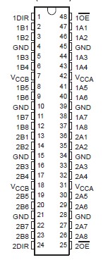 Specifications
| Supply voltage range, VCCA and VCCB |
−0.5 V to 4.6 V |
Input voltage range, VI (see Note 1):
I/O ports (A port)
I/O ports (B port)
Control inputs |
−0.5 V to 4.6 V
−0.5 V to 4.6 V
−0.5 V to 4.6 V |
Voltage range applied to any output in the high-impedance or power-off state, VO
(see Note 1): (A port)
(B port) |
−0.5 V to 4.6 V
−0.5 V to 4.6 V |
Voltage range applied to any output in the high or low state, VO
(see Notes 1 and 2): (A port)
(B port) |
−0.5 V to VCCA + 0.5 V
−0.5 V to VCCB + 0.5 V |
| Input clamp current, IIK (VI < 0) |
−50 mA |
| Output clamp current, IOK (VO < 0) |
−50 mA |
| Continuous output current, IO |
±50 mA |
| Continuous current through VCCA, VCCB, or GND |
±100 mA |
Package thermal impedance, JA (see Note 3): DGG package
DGV package
GQL/ZQL package |
70/W
58/W
28/W |
| Storage temperature range, Tstg |
−65 to 150 |
NOTES:
1. The input and output negative-voltage ratings may be exceeded if the input and output current ratings areobserved.
2. The output positive-voltage rating may be exceeded up to 4.6 V maximum if the output current rating is observed.
3. The package thermal impedance is calculated in accordance with JESD 51-7.
DescriptionThis SN74AVCB164245 16-bit (dual-octal) noninverting bus transceiver uses two separate configurable power-supply rails. The A port is designed to track VCCA. VCCA accepts any supply voltage from 1.4 V to 3.6 V. The B port is designed to track VCCB. VCCB accepts any supply voltage from 1.4 V to 3.6 V. This allows for universal low-voltage bidirectional translation between any of the 1.5-V, 1.8-V, 2.5-V, and 3.3-V voltage nodes.
The SN74AVCB164245 is designed for asynchronous communication between data buses. The device transmits data from the A bus to the B bus or from the B bus to the A bus, depending on the logic level at the direction-control (DIR) input. The output-enable (OE) input can be used to disable the outputs so the buses are effectively isolated.
The SN74AVCB164245 is designed so that the control pins (1DIR, 2DIR, 1OE, and 2OE) are supplied by VCCB. To ensure the high-impedance state during power up or power down, OE should be tied to VCCB through a pullup resistor; the minimum value of the resistor is determined by the current-sinking capability of the driver.
This SN74AVCB164245 device is fully specified for partial-power-down applications using Ioff. The Ioff circuitry disables the outputs, preventing damaging current backflow through the device when it is powered down. If either VCC input is at GND, both ports are in the high-impedance state.

 SN74AVCB164245 Data Sheet


