Pinout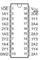 SpecificationsSupply voltage range, VCC . . . . . . . . . . . . . . . . . . . . . . . . . . . . . . . . . . . . . . . . . 0.5 V to 7 V
Input voltage range, VI (see Note 1) . . . . . . . . . . . . . . . . . . . . . . . . . . . . . . . . . 0.5 V to 7 V
Voltage range applied to any output in the disabled or power-off state, VO. . 0.5 V to 5.5 V
Voltage range applied to any output in the high state, VO. . . . . . . . . . . . . . . . . 0.5 V to VCC
Input clamp current, IIK . . . . . . . . . . . . . . . . . . . . . . . . . . . . . . . . . . . . . . . . . . . . . . . . 30 mA
Current into any output in the low state . . . . . . . . . . . . . . . . . . . . . . . . . . . . . . . . . . . . 24 mA
Operating free-air temperature range: SN54BCT2240 . . . . . . . . . . . . . . . . . 55°C to 125°C
SN74BCT2240 . . . . . . . . . . . . . . . . . . . . . 0°C to 70°C
Storage temperature range. . . . . . . . . . . . . . . . . . . . . . . . . . . . . . . . . . . . . . 65°C to 150°CDescriptionThese octal buffers and line drivers SN74BCT2240 are designed specifically to improve both the performance and density of 3-state memory address drivers, clock drivers, and bus-oriented receivers and transmitters. Taken together with the SN74BCT2241 and BCT2244, these devices provide the choice of selected combinations of inverting and coninverting outputs, symmetrical active-low output-enable (OE) inputs, and complementary OE and OE inputs. These devices feature high fan-out and improved fan-in.
The BCT2240 is organized as two 4-bit line drivers with separate output-enable (OE) inputs. When OE is low, the device passes data from the A inputs to the Y outputs. When OE is high, the outputs are in the high-impedance state.
The SN74BCT2240 outputs, which are designed to source or sink up to 12 mA, include 33-W series resistors to reduce overshoot and undershoot.
The SN54BCT2240 is characterized for operation over the full military temperature range of 55°C to 125°C. The SN74BCT2240 is characterized for operation from 0°C to 70°C.

 SN74BCT2240 Data Sheet


