SN74BCT29833

Features: • BiCMOS Process With TTL Inputs and Outputs• BiCMOS Design Reduces Standby Current• Flow-Through Pinout (All Inputs on Opposite Side From Outputs)• Functionally Equivalent to SN74ALS29833 and AMD Am29833• High-Speed Bus Transceiver With Parity Generator/Che...

product image

SN74BCT29833 Picture
SeekIC No. : 004498605 Detail

SN74BCT29833: Features: • BiCMOS Process With TTL Inputs and Outputs• BiCMOS Design Reduces Standby Current• Flow-Through Pinout (All Inputs on Opposite Side From Outputs)• Functionally Eq...

floor Price/Ceiling Price

Part Number:
SN74BCT29833
Supply Ability:
5000

Price Break

  • Qty
  • 1~5000
  • Unit Price
  • Negotiable
  • Processing time
  • 15 Days
Total Cost: $ 0.00

SeekIC Buyer Protection PLUS - newly updated for 2013!

  • Escrow Protection.
  • Guaranteed refunds.
  • Secure payments.
  • Learn more >>

Month Sales

268 Transactions

Rating

evaluate  (4.8 stars)

Upload time: 2025/12/24

Payment Methods

All payment methods are secure and covered by SeekIC Buyer Protection PLUS.

Notice: When you place an order, your payment is made to SeekIC and not to your seller. SeekIC only pays the seller after confirming you have received your order. We will also never share your payment details with your seller.
Product Details

Description


Features:

• BiCMOS Process With TTL Inputs and Outputs
• BiCMOS Design Reduces Standby Current
• Flow-Through Pinout (All Inputs on Opposite Side From Outputs)
• Functionally Equivalent to SN74ALS29833 and AMD Am29833
• High-Speed Bus Transceiver With Parity Generator/Checker
• Parity-Error Flag With Open-Collector Output
• Available Register For Storage of the Parity-Error Flag
• Package Options Include Plastic Small-Outline (DW) Packages and Standard Plastic 300-mil DIPs (NT)


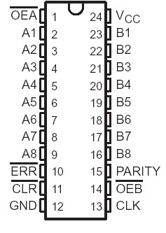
Pinout

  Connection Diagram


Specifications

Supply voltage, VCC . . . . . . . . . . . . . . . . . . . . . . . . . . . . . . . . . . . . . . . . . . . . . . . . . .  .7 V
Input voltage, VI. . . . . . . . . . . . . . . . . . . . . . . . . . . . . . . . . . . . . . . . . . . . . . . . . . . . . . 7 V
Voltage applied to a disabled I/O port  . . . . . . . . . . . . . . . . . . . . . . . . . . . . . . . . . . . 5.5 V
Operating free-air temperature range . . . . . . . . . . . . . . . . . . . . . . . . . . . . .  . 0°C to 70°C
Storage temperature range  . . . . . . . . . . . . . . . . . . . . . . . . . . . . . . . . . . . . 65°C to 150°C


Description

The SN74BCT29833 is an 8-bit to 9-bit parity transceiver designed for asynchronous communication between data buses. When data is transmitted from the A to B bus, a parity bit is generated. When data is transmitted from the B to A bus with its corresponding parity bit, the parity-error (ERR) output will indicate whether or not an error in the B data has occurred. The output-enable (OEA, OEB) inputs can be used to disable the device so that the buses are effectively isolated.

A 9-bit parity generator/checker generates a parity-odd (PARITY) output and monitors the parity of the I/O ports with an open-collector parity-error (ERR) flag. ERR is clocked into the register on the rising edge of the CLK input. The error flag register is cleared with a low pulse on the clear (CLR) input. When both OEA and OEB are low, data is transferred from the A bus to the B bus and inverted parity is generated. Inverted parity is a forced error condition which gives the designer more system diagnostic capability. The SN74BCT29833 provides true logic.

The SN74BCT29833 is characterized for operation from 0°C to 70°C.


Customers Who Bought This Item Also Bought

Margin,quality,low-cost products with low minimum orders. Secure your online payments with SeekIC Buyer Protection.
Computers, Office - Components, Accessories
Crystals and Oscillators
Optoelectronics
Cable Assemblies
Static Control, ESD, Clean Room Products
View more