Features: • State-of-the-Art BiCMOS Design Significantly Reduces ICCZ• Full Parallel Access for Loading• 3-State Inverting Outputs Drive Bus Lines or Buffer Memory Address Registers• ESD Protection Exceeds 2000 V Per MIL-Std-883C, Method 3015• Package Options Include ...
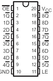
SN74BCT533: Features: • State-of-the-Art BiCMOS Design Significantly Reduces ICCZ• Full Parallel Access for Loading• 3-State Inverting Outputs Drive Bus Lines or Buffer Memory Address Register...
SeekIC Buyer Protection PLUS - newly updated for 2013!
268 Transactions
All payment methods are secure and covered by SeekIC Buyer Protection PLUS.

The SN74BCT533 is an 8-bit transparent D-type latch with 3-state outputs designed specifically for driving highly capacitive or relatively low-impedance loads. It is particularly suitable for implementing buffer registers, I/O ports, bidirectional bus drivers, and working registers.
When the latch-enable (LE) input is high, the Q outputs follow the complements of the data (D) inputs. When LE is taken low, the Q outputs are latched at the inverse of the levels set up at the D inputs. The SN74BCT533 provides inverted data at its outputs.
A buffered output-enable (OE) input of the SN74BCT533 can be used to place the eight outputs in either a normal logic state (high or low logic levels) or a high-impedance state. In the high-impedance state, the outputs neither load nor drive the bus lines significantly. The high-impedance state and the increased drive provide the capability to drive bus lines without need for interface or pullup components.
The output-enable (OE) input of the SN74BCT533 does not affect the internal operations of the latch. Previously stored data can be retained or new data can be entered while the outputs are in the high-impedance state.
The SN74BCT533 is characterized for operation from 0°C to 70°C.