Features: ` Member of the Texas Instruments Widebus™ Family
` High-Bandwidth Data Path (up to 500 MHz (1))
` 5-V Tolerant I/Os With Device Powered Up or Powered Down
` Low and Flat ON-State Resistance (ron) Characteristics Over Operating Range (ron = 5 Typ)
` Rail-to-Rail Switching on Data I/O Ports
0- to 5-V Switching With 3.3-V VCC
0- to 3.3-V Switching With 2.5-V VCC
` Bidirectional Data Flow With Near-Zero Propagation Delay
` Low Input/Output Capacitance Minimizes Loading and Signal Distortion (Cio(OFF) = 4 pF Typ)
` Fast Switching Frequency (fOE = 20 MHz Max)
` Data and Control Inputs Provide Undershoot Clamp Diodes
` Low Power Consumption (ICC = 1 mA Typ)
` VCC Operating Range From 2.3 V to 3.6 V
` Data I/Os Support 0- to 5-V Signaling Levels (0.8 V, 1.2 V, 1.5 V, 1.8 V, 2.5 V, 3.3 V, 5 V)
` Control Inputs Can Be Driven by TTL or 5-V/3.3-V CMOS Outputs
` Ioff Supports Partial-Power-Down Mode Operation
` Latch-Up Performance Exceeds 100 mA Per JESD 78, Class II
1000-V Charged-Device Model (C101)
` Supports Both Digital and Analog Applications: PCI Interface, Differential Signal Interface, Memory
Interleaving, Bus Isolation, Low-Distortion Signal GatingPinout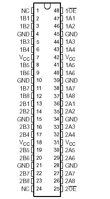 Specifications
| |
Min |
Max |
Unit |
|
VCC |
Supply voltage range |
-0.5 |
4.6 |
V |
|
VIN |
Control input voltage range(2) (3) |
-0.5 |
7 |
V |
|
VI/O |
Switch I/O voltage range(2) (3) (4) |
-0.5 |
7 |
V |
|
IIK |
Control input clamp current |
VIN < 0 |
|
50 |
mA |
|
II/OK |
I/O port clamp current |
VI/O < 0 |
|
-50 |
mA |
|
II/O |
ON-state switch current(5) |
|
±64 |
mA |
| |
Continuous current through VCC or GND |
|
±100 |
mA |
|
JA |
Package thermal impedance(6) |
DGG package |
|
70 |
/W |
| DGV package |
58 |
| DL package |
63 |
|
Tstg |
storage temperature |
|
-65 |
150 |
|
(1) Stresses beyond those listed under "absolute maximum ratings" may cause permanent damage to the
device. These are stress ratings only, and functional operation of the device at these or any other
conditions beyond those indicated under "recommended operating conditions" is not implied. Exposure
to absolute-maximum-rated conditions for extended periods may affect device reliability.
(2) All voltages are with respect to ground unless otherwise specified.
(3) The input and output voltage ratings may be exceeded if the input and output clamp-current ratings
are observed.
(4) VI and V
O are used to denote specific conditions for V
I/O.
(5) II and I
O are used to denote specific conditions for I
I/O.
(6) The package thermal impedance is calculated in accordance with JESD 51-7.
DescriptionThe SN74CB3Q16245 is a high-bandwidth FET bus switch utilizing a charge pump to elevate the gate voltage of the pass transistor, providing a low and flat ON-state resistance (ron). The low and flat ON-state resistance allows for minimal propagation delay and supports rail-to-rail switching on the data input/output (I/O) ports. The device also features low data I/O capacitance to minimize capacitive loading and signal distortion on the data bus. Specifically designed to support high-bandwidth applications, the SN74CB3Q16245 provides an optimized interface solution ideally suited for broadband communications, networking, and data-intensive computing systems.
The SN74CB3Q16245 is organized as two 8-bit bus switches with separate output-enable (1OE, 2OE) inputs. It can be used as two 8-bit bus switches, or as one 16-bit bus switch. When OE is low, the associated 8-bit bus switch is ON, and the A port is connected to the B port, allowing bidirectional data flow between ports. When OE is high, the associated 8-bit bus switch is OFF, and a high-impedance state exists between the A and B ports.
This SN74CB3Q16245 is fully specified for partial-power-down applications using Ioff. The Ioff circuitry prevents damaging current backflow through the device when it is powered down. The device has isolation during power off.
To ensure the high-impedance state during power up or power down, OE should be tied to VCC through a pullup resistor; the minimum value of the resistor is determined by the current-sinking capability of the driver.

 SN74CB3Q16245 Data Sheet


