Pinout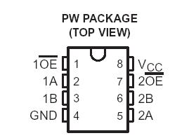 Specifications
Supply voltage range, VCC. . . . . . . . . . . . . . . . . . . . . . . . . . . . . . . . . . . . . . . . . . . . .. .. . −0.5 V to 4.6 V
Control input voltage range, VIN (see Notes 1 and 2) . . . . . . . . . . . . . . . . .. . . . . .. . . .. . . .−0.5 V to 7 V.
Switch I/O voltage range, VI/O (see Notes 1, 2, and 3). . . . . . . . . . . . . . . . . . . . . . .. .. . . . −0.5 V to 7 V
.
Control input clamp current, IIK(VIN < 0) . . . . . . . . . . . . . . . . . . . . . . . . . . . . . . . . . . . . . . . .. . . .−50 mA
I/O port clamp current, II/OK (VI/O < 0) . . . . . . . . . . . . . . . . . . . . . . . . .. . . . . . . . . . . . . . . . . . . .−50 mA
ON-state switch current, II/O (see Note 4) . . . . . . . . . . . . . . . . . . . . . . . . . . . . . . . . . . . . . . . . . .±64 mA
Continuous current through VCC or GND terminals . . . . . . . . . . . . . . . . . . . . . . . . . . . . . . . . . .±100 mA
Package thermal impedance, JA (see Note 5) . . . . . . . . . . . . . . . . . . . . . . . . . . . . . . . . . . . . . .88°C/W
Storage temperature range, Tstg . . . . . . . . . . . . . . . . . . . . . . . . . . . . . . . . . . . . . . . .−65°C to 150°C
DescriptionThe SN74CB3Q3306A is a high-bandwidth FET bus switch utilizing a charge pump to elevate the gate voltageof the pass transistor, providing a low and flat ON-state resistance (ron). The low and flat ON-state resistance allows for minimal propagation delay and supports rail-to-rail switching on the data input/output (I/O) ports. The device also features low data I/O capacitance to minimize capacitive loading and signal distortion on the data bus. Specifically designed to support high-bandwidth applications, the SN74CB3Q3306A provides anoptimized interface solution ideally suited for broadband communications, networking, and data-intensive computing systems.

 SN74CB3Q3306A Data Sheet


