Features: ` Member of the Texas Instruments Widebus™ Family
` Output Voltage Translation Tracks VCC
` Supports Mixed-Mode Signal Operation on All Data I/O Ports
5-V Input Down to 3.3-V Output Level Shift With 3.3-V VCC
5-V/3.3-V Input Down to 2.5-V Output Level Shift With 2.5-V VCC
` 5-V-Tolerant I/Os With Device Powered Up or Powered Down
` Bidirectional Data Flow With Near-Zero Propagation Delay
` Low ON-State Resistance (ron) Characteristics (ron = 5 W Typ)
` Low Input/Output Capacitance Minimizes Loading (Cio(OFF) = 5 pF Typ)
` Data and Control Inputs Provide Undershoot Clamp Diodes
` Low Power Consumption (ICC = 40 mA Max)
` VCC Operating Range From 2.3 V to 3.6 V
` Data I/Os Support 0- to 5-V Signaling Levels (0.8 V, 1.2 V, 1.5 V, 1.8 V, 2.5 V, 3.3 V, 5 V)
` Control Inputs Can Be Driven by TTL or 5-V/3.3-V CMOS Outputs
` Ioff Supports Partial-Power-Down Mode Operation
` Latch-Up Performance Exceeds 250 mA Per JESD 17
` ESD Performance Tested Per JESD 22
2000-V Human-Body Model (A114-B, Class II)
1000-V Charged-Device Model (C101)
` Supports Digital Applications: Level Translation, PCI Interface, USB Interface, Memory Interleaving, and Bus Isolation
` Ideal for Low-Power Portable EquipmentApplicationAudio
Automotive
Broadband
Digital Control
Military
Optical Networking
Security
Telephony
Video & Imaging
WirelessPinout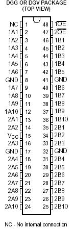 Specifications
| |
|
|
MIN |
MAX |
UNIT |
| VCC |
Supply voltage range |
|
0.5 |
7 |
V |
| VIN |
Control input voltage range(2) (3) |
|
0.5 |
7 |
V |
| VI/O |
Switch I/O voltage range(2) (3) (4) |
|
0.5 |
7 |
V |
| IIK |
Control input clamp current |
VIN < 0 |
|
50 |
mA |
| II/OK |
I/O port clamp current |
VI/O < 0 |
|
50 |
mA |
| IIO |
ON-state switch current(5) |
|
|
±128 |
mA |
| |
Continuous current through VCC or GND |
|
|
±100 |
mA |
qJA
|
Package thermal impedance(6) |
DGG package |
|
70 |
°C/W |
| DGV package |
|
58 |
| Tstg |
Storage temperature range |
|
65 |
150 |
°C |
Description The SN74CB3T16210 is a high-speed TTL-compatible FET bus switch with low ON-state resistance (r
on), allowing for minimal propagation delay. The device fully supports mixed-mode signal operation on all data I/O ports by providing voltage translation that tracks V
CC. The SN74CB3T16210 supports systems using 5-V TTL, 3.3-V LVTTL, and 2.5-V CMOS switching standards, as well as user-defined switching levels (see Figure 1).
The SN74CB3T16210 is organized as two 10-bit bus switches with separate ouput-enable (1OE, 2OE) inputs. It can be used as two 10-bit bus switches or as one 20-bit bus switch. When OE is low, the associated 10-bit bus switch is ON, and the A port is connected to the B port, allowing bidirectional data flow between ports. When OE is high, the associated 10-bit bus switch is OFF, and a high-impedance state exists between the A and B ports.
This SN74CB3T16210 device is fully specified for partial-power-down applications using I
off. The Ioff feature ensures that damaging current will not backflow through the device when it is powered down. The device has isolation during power off.
To ensure the SN74CB3T16210 high-impedance state during power up or power down, OE should be tied to V
CC through a pullup resistor; the minimum value of the resistor is determined by the current-sinking capability of the driver.

 SN74CB3T16210 Data Sheet


