Maximum Operating Temperature
: + 85 C
Minimum Operating Temperature
: - 40 C
Packaging
: Reel
Propagation Delay Time
: 0.15 ns
Number of Switches
: 8
Package / Case
: VQFN-20
Features: ` Undershoot Protection for Off-Isolation on A and B Ports Up To −2 V
` Bidirectional Data Flow, With Near-Zero Propagation Delay
` Low ON-State Resistance (ron) Characteristics (ron = 3 Typical)
` Low Input/Output Capacitance Minimizes Loading and Signal Distortion
(Cio(OFF) = 5.5 pF Typical)
` Data and Control Inputs Provide Undershoot Clamp Diodes
` Low Power Consumption
(ICC = 3 A Max)
` VCC Operating Range From 4 V to 5.5 V
` Data I/Os Support 0 to 5-V Signaling Levels
(0.8-V, 1.2-V, 1.5-V, 1.8-V, 2.5-V, 3.3-V, 5-V)
` Control Inputs Can Be Driven by TTL or 5-V/3.3-V CMOS Outputs
` Ioff Supports Partial-Power-Down Mode Operation
` Latch-Up Performance Exceeds 100 mA Per JESD 78, Class II
` ESD Performance Tested Per JESD 22
− 2000-V Human-Body Model
(A114-B, Class II)
− 1000-V Charged-Device Model (C101)
` Supports Both Digital and Analog
Applications: USB Interface, Memory Interleaving, Bus Isolation, Low-Distortion Signal Gating
Pinout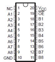 Specifications
Supply voltage range, VCC ................................................................. −0.5 V to 7 V
Control input voltage range, VIN (see Notes 1 and 2)........................ −0.5 V to 7 V
Switch I/O voltage range, VI/O (see Notes 1, 2, and 3) ...................... −0.5 V to 7 V
Control input clamp current, IIK (VIN < 0) .................................................... −50 mA
I/O port clamp current, II/OK (VI/O < 0) ........................................................ −50 mA
ON-state switch current, II/O (see Note 4)................................................ . ±128 mA
Continuous current through VCC or GND terminals ......................................±100 mA
Package thermal impedance, JA (see Note 5): DB package ........................ 70°C/W
(see Note 5): DBQ package.........................68°C/W
(see Note 5): DGV package .......................92°C/W
(see Note 5): DW package ........................58°C/W
(see Note 5): PW package ........................83°C/W
(see Note 6): RGY package ...................... 37°C/W
Storage temperature range, Tstg ....................................................−65°C to 150°C
‡ Stresses beyond those listed under "absolute maximum ratings" may cause permanent damage to the device. These are stress ratings only, and functional operation of the device at these or any other conditions beyond those indicated under "recommended operating conditions" is not implied. Exposure to absolute-maximum-rated conditions for extended periods may affect device reliability.
NOTES: 1. All voltages are with respect to ground unless otherwise specified.
2. The input and output voltage ratings may be exceeded if the input and output clamp-current ratings are observed.
3. VI and VO are used to denote specific conditions for VI/O.
4. II and IO are used to denote specific conditions for II/O.
5. The package thermal impedance is calculated in accordance with JESD 51-7.
6. The package thermal impedance is calculated in accordance with JESD 51-5.
DescriptionThe SN74CBT3245CRGYR is a high-speed TTL-compatible FET bus switch with low ON-state resistance (ron),allowing for minimal propagation delay. Active Undershoot-Protection Circuitry on the A and B ports of the SN74CBT3245C provides protection for undershoot up to −2 V by sensing an undershoot event and ensuring that the switch remains in the proper OFF state.
The SN74CBT3245CRGYR is organized as an 8-bit bus switch with a single output-enable (OE) input. When OE is low, the bus switch is ON, and the A port is connected to the B port, allowing bidirectional data flow between ports. When OE is high, the bus switch is OFF, and the high-impedance state exists between the A and B ports.
Parameters: | Technical/Catalog Information | SN74CBT3245CRGYR |
| Vendor | Texas Instruments (VA) |
| Category | Integrated Circuits (ICs) |
| Circuit | 8 x 1:1 |
| Independent Circuits | 1 |
| Mounting Type | Surface Mount |
| Current - Output High, Low | 15mA, 64mA |
| Package / Case | 20-VQFN |
| Packaging | Cut Tape (CT) |
| Type | FET Bus Switch |
| Voltage Supply Source | Single Supply |
| Operating Temperature | -40°C ~ 85°C |
| Voltage - Supply | 4.5 V ~ 5.5 V |
| Drawing Number | 296; 4203539-4; RGY; 20 |
| Lead Free Status | Lead Free |
| RoHS Status | RoHS Compliant |
| Other Names | SN74CBT3245CRGYR
SN74CBT3245CRGYR
296 19203 1 ND
296192031ND
296-19203-1
|

 SN74CBT3245CRGYR Data Sheet


