SN74CBT3305C

Features: · Undershoot Protection for Off-Isolation on A and B Ports Up To −2 V· Bidirectional Data Flow, With Near-Zero Propagation Delay· Low ON-State Resistance (ron) Characteristics (ron = 3 Ω Typical)· Low Input/Output Capacitance Minimizes Loading and Signal Distortion (Cio(OFF) ...

product image

SN74CBT3305C Picture
SeekIC No. : 004498714 Detail

SN74CBT3305C: Features: · Undershoot Protection for Off-Isolation on A and B Ports Up To −2 V· Bidirectional Data Flow, With Near-Zero Propagation Delay· Low ON-State Resistance (ron) Characteristics (ron =...

floor Price/Ceiling Price

Part Number:
SN74CBT3305C
Supply Ability:
5000

Price Break

  • Qty
  • 1~5000
  • Unit Price
  • Negotiable
  • Processing time
  • 15 Days
Total Cost: $ 0.00

SeekIC Buyer Protection PLUS - newly updated for 2013!

  • Escrow Protection.
  • Guaranteed refunds.
  • Secure payments.
  • Learn more >>

Month Sales

268 Transactions

Rating

evaluate  (4.8 stars)

Upload time: 2025/12/24

Payment Methods

All payment methods are secure and covered by SeekIC Buyer Protection PLUS.

Notice: When you place an order, your payment is made to SeekIC and not to your seller. SeekIC only pays the seller after confirming you have received your order. We will also never share your payment details with your seller.
Product Details

Description


Features:

· Undershoot Protection for Off-Isolation on A and B Ports Up To −2 V
· Bidirectional Data Flow, With Near-Zero Propagation Delay
· Low ON-State Resistance (ron) Characteristics (ron = 3 Ω Typical)
· Low Input/Output Capacitance Minimizes Loading and Signal Distortion (Cio(OFF) = 5 pF Typical)
· Data and Control Inputs Provide Undershoot Clamp Diodes
· Low Power Consumption (ICC = 3 µA Max)
· VCC Operating Range From 4 V to 5.5 V
· Data I/Os Support 0 to 5-V Signaling Levels (0.8-V, 1.2-V, 1.5-V, 1.8-V, 2.5-V, 3.3-V, 5-V)
· Control Inputs Can Be Driven by TTL or 5-V/3.3-V CMOS Outputs
· Ioff Supports Partial-Power-Down Mode Operation
· Latch-Up Performance Exceeds 100 mA Per JESD 78, Class II
· ESD Performance Tested Per JESD 22
   − 2000-V Human-Body Model (A114-B, Class II)
   − 1000-V Charged-Device Model (C101)
· Supports Both Digital and Analog Applications: USB Interface, Bus Isolation, Low-Distortion Signal Gating


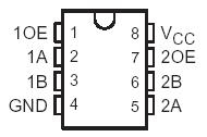
Pinout

  Connection Diagram


Specifications

Supply voltage range, VCC . . . . . . . . . . . . . . . . . . . . . . . . . . . .. .−0.5 V to 7 V
Control input voltage range, VIN (see Notes 1 and 2) . . . . . . . . .−0.5 V to 7 V
Switch I/O voltage range, VI/O (see Notes 1, 2, and 3) . . . . . . . .−0.5 V to 7 V
Control input clamp current, IIK (VIN < 0) . . . . . . . . . . . . . . . . . . . . . . .−50 mA
I/O port clamp current, II/OK (VI/O < 0) . . . . . . . . . . . . . . . . . . . . . . .. .−50 mA
ON-state switch current, II/O (see Note 4) . . . . . . . . . . . . . . . . . . . . .±128 mA
Continuous current through VCC or GND terminals . . . . . . . . ... . . . . .±100 mA
Package thermal impedance, JA (see Note 5): D package . .. . .. . . . .97°C/W 
                                                                          PW package . .. . .. . .149°C/W
Storage temperature range, Tstg . . . . . . . . . . . . . . . . .  . . . .−65°C to 150°C


Description

The SN74CBT3305C is a high-speed TTL-compatible FET bus switch with low ON-state resistance (ron), allowing for minimal propagation delay. Active Undershoot-Protection Circuitry on the A and B ports of the SN74CBT3305C provides protection for undershoot up to −2 V by sensing an undershoot event and ensuring that the switch remains in the proper OFF state.

The SN74CBT3305C is organized as two 1-bit bus switches with separate output-enable (1OE, 2OE) inputs. It can be used as two 1-bit bus switches or as one 2-bit bus switch. When OE is high, the associated 1-bit bus switch is ON, and the A port is connected to the B port, allowing bidirectional data flow between ports. When OE is low, the associated 1-bit bus switch is OFF, and the high-impedance state exists between the A and B ports.

This SN74CBT3305C is fully specified for partial-power-down applications using Ioff. The Ioff feature ensures that damaging current will not backflow through the device when it is powered down. The device has isolation during power off.


To ensure the high-impedance state of the SN74CBT3305C during power up or power down, OE should be tied to GND through a pulldown resistor; the minimum value of the resistor is determined by the current-sourcing capability of the driver.


Customers Who Bought This Item Also Bought

Margin,quality,low-cost products with low minimum orders. Secure your online payments with SeekIC Buyer Protection.
Soldering, Desoldering, Rework Products
Power Supplies - Board Mount
Boxes, Enclosures, Racks
Crystals and Oscillators
Isolators
View more