Features: ` Standard '245-Type Pinout
` 5- Switch Connection Between Two Ports
` TTL-Compatible Input Levels
` Package Options Include Plastic Shrink Small-Outline (DB), Thin Very Small-Outline (DGV), Small-Outline (DW), and Thin Shrink Small-Outline (PW) Packages
Pinout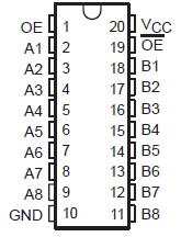 Specifications
Supply voltage range, VCC . . . . . . . . . . . . . . . . . . . . . . . . . . . . . . . . . . . . . . . . . 0.5 V to 7 V
Input voltage range, VI (see Note 1) . . . . . . . . . . . . . . . . . . . . . . . . . . . . . . . . 0.5 V to 7 V
Continuous channel current . . . . . . . . . . . . . . . . . . . . . . . . . . . . . . . . . . . . . . . . . . . . . 128 mA
Input clamp current, IIK (VI/O < 0) . . . . . . . . . . . . . . . . . . . . . . . . . . . . . . . . . . . . . . . 50 mA
Package thermal impedance, JA (see Note 2): DB package . . . . . . . . . . . . . . . . . . . . 115°C
DGV package . . . . . . . . . . . . . . . . . . . 146°C
DW package . . . . . . . . . . . . . . . . . . . . . 97°C
PW package . . . . . . . . . . . . . . . . . . . . 128°C
Storage temperature range, Tstg . . . . . . . . . . . . . . . . . . . . . . . . .. . . . . . . . 65°C to 150°C
† Stresses beyond those listed under "absolute maximum ratings" may cause permanent damage to the device. These are stress ratings only, and functional operation of the device at these or any other conditions beyond those indicated under "recommended operating conditions" is not implied. Exposure to absolute-maximum-rated conditions for extended periods may affect device reliability.
NOTES: 1. The input and output negative-voltage ratings may be exceeded if the input and output clamp-current ratings are observed.
2. The package thermal impedance is calculated in accordance with JESD 51.
DescriptionThe SN74CBT3345 provides eight bits of high-speed TTL-compatible bus switching in a standard '245 device pinout. The low on-state resistance of the switch allows connections to be made with minimal propagation delay.
The SN74CBT3345 is organized as one 8-bit switch bank with dual output-enable (OE and OE) inputs. When OE is low or OE is high, the switch is on and port A is connected to port B. When OE is high and OE is low, the switch is open and a high-impedance state exists between the two ports.
The SN74CBT3345 is characterized for operation from 0°C to 70°C.

 SN74CBT3345 Data Sheet


