Features: ` Member of the Texas Instruments WidebusTM Family
` Undershoot Protection for Off-Isolation on A and B Ports Up to −2 V
` B-Port Outputs Are Precharged by Bias Voltage (BIASV) to Minimize Signal Distortion During Live Insertion and Hot-Plugging
` Supports PCI Hot Plug
` Bidirectional Data Flow, With Near-Zero Propagation Delay
` Low ON-State Resistance (ron) Characteristics (ron = 3 Typical)
` Low Input/Output Capacitance Minimizes Loading and Signal Distortion (Cio(OFF) = 5.5 pF Typical)
` Data and Control Inputs Provide Undershoot Clamp Diodes
` Low Power Consumption (ICC = 3 A Max)
` VCC Operating Range From 4 V to 5.5 V
` Data I/Os Support 0 to 5-V Signaling Levels (0.8-V, 1.2-V, 1.5-V, 1.8-V, 2.5-V, 3.3-V, 5-V)
` Control Inputs Can be Driven by TTL or 5-V/3.3-V CMOS Outputs
` Ioff Supports Partial-Power-Down Mode Operation
` Latch-Up Performance Exceeds 100 mA Per JESD 78, Class II
` ESD Performance Tested Per JESD 22
− 2000-V Human-Body Model (A114-B, Class II)
− 1000-V Charged-Device Model (C101)
` Supports Both Digital and Analog
Applications: PCI Interface, Memory Interleaving, Bus Isolation, Low-Distortion Signal Gating
Pinout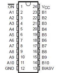 Specifications
Supply voltage range, VCC . . . . . . . . . . . . . . . . . . . . . . . . . . .. −0.5 V to 7 V
Bias supply voltage range, BIASV . . . . . . . . . . . . . . . . . . . . . .. −0.5 V to 7 V
Control input voltage range, VIN (see Notes 1 and 2) . . . . . . . −0.5 V to 7 V
Switch I/O voltage range, VI/O (see Notes 1, 2, and 3) . . . . . . −0.5 V to 7 V
Control input clamp current, IIK (VIN < 0) . . . . . . . . . . . . . . . . . . . . −50 mA
I/O port clamp current, II/OK (VI/O < 0) . . . . . . . . . . . . . . . . . . . . . . −50 mA
ON-state switch current, II/O (see Note 4) . . . . . . . . . . . . . . . . . . . ±128 mA
Continuous current through VCC or GND terminals . . . . . . . . . . . . . ±100 mA
Package thermal impedance, JA (see Note 5): DB package . . . . .. . 63°C/W
DBQ package . . . . . . 61°C/W
DGV package . . . . . . 86°C/W
DW package . . . . . . 46°C/W
PW package . . . . . . . 88°C/W
Storage temperature range, Tstg . . . . . . . . . . . . . . . . . . . . −65°C to 150°C
† Stresses beyond those listed under "absolute maximum ratings" may cause permanent damage to the device. These are stress ratings only, and functional operation of the device at these or any other conditions beyond those indicated under "recommended operating conditions" is not implied. Exposure to absolute-maximum-rated conditions for extended periods may affect device reliability.
NOTES: 1. All voltages are with respect to ground unless otherwise specified.
2. The input and output voltage ratings may be exceeded if the input and output clamp-current ratings are observed.
3. VI and VO are used to denote specific conditions for VI/O.
4. II and IO are used to denote specific conditions for II/O.
5. The package thermal impedance is calculated in accordance with JESD 51-7.
DescriptionThe SN74CBT6800C is a high-speed TTL-compatible FET bus switch with low ON-state resistance (ron),allowing for minimal propagation delay. Active Undershoot-Protection Circuitry on the A and B ports of the SN74CBT6800C provides protection for undershoot up to −2 V by sensing an undershoot event and ensuring that the switch remains in the proper OFF state. The device also precharges the B port to a user-selectable bias voltage (BIASV) to minimize live-insertion noise.
The SN74CBT6800C is a 10-bit bus switch with a single output-enable (ON) input. When ON is low, the 10-bit bus switch is ON, and the A port is connected to the B port, allowing bidirectional data flow between ports. When ON is high, the 10-bit bus switch is OFF, and a high-impedance state exists between the A and B ports. The B port is precharged to BIASV through the equivalent of a 10-k resistor when ON is high, or if the device is powered down (VCC = 0 V).
During insertion (or removal) of a card into (or from) an active bus, the card's output voltage may be close to GND. When the SN74CBT6800C connector pins make contact, the card's parasitic capacitance tries to force the bus signal to GND, creating a possible glitch on the active bus. This glitching effect can be reduced by using a bus switch with precharged bias voltage (BIASV) of the bus switch equal to the input threshold voltage level of the receivers on the active bus. This method will ensure that any glitch produced by insertion (or removal) of the card will not cross the input threshold region of the receivers on the active bus, minimizing the effects of live-insertion noise.
This SN74CBT6800C device is fully specified for partial-power-down applications using Ioff. The Ioff feature ensures that damaging current will not backflow through the device when it is powered down. The device has isolation during power off.
To ensure the high-impedance state during power up or power down, ON should be tied to VCC through a pullup resistor; the minimum value of the resistor is determined by the current-sinking capability of the driver.

 SN74CBT6800C Data Sheet


