Features: · Undershoot Protection for Off-Isolation on A and B Ports Up To −2 V
· Integrated Diode to VCC Provides 5-V Input Down To 3.3-V Output Level Shift
· Bidirectional Data Flow, With Near-Zero Propagation Delay
· Low ON-State Resistance (ron) Characteristics (ron = 3 Ω Typical)
· Low Input/Output Capacitance Minimizes Loading and Signal Distortion (Cio(OFF) = 5 pF Typical)
· Data and Control Inputs Provide Undershoot Clamp Diodes
· VCC Operating Range From 4.5 V to 5.5 V
· Data I/Os Support 0 to 5-V Signaling Levels (0.8-V, 1.2-V, 1.5-V, 1.8-V, 2.5-V, 3.3-V, 5-V)
· Control Inputs Can be Driven by TTL or 5-V/3.3-V CMOS Outputs
· Ioff Supports Partial-Power-Down Mode Operation
· Latch-Up Performance Exceeds 100 mA Per JESD 78, Class II
· ESD Performance Tested Per JESD 22
− 2000-V Human-Body Model (A114-B, Class II)
− 1000-V Charged-Device Model (C101)
· Supports Both Digital and Analog Applications: USB Interface, Memory Interleaving, Bus Isolation, Low-Distortion Signal GatingPinout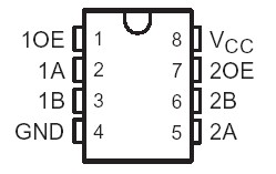 Specifications
Supply voltage range, . . . . . . . . . . . . . . . . . . . . . . . . . . . . . . . . . . . . . . . . . . . . . . . . . . . . . .VCC −0.5 V to 7 V
Control input voltage range, VIN (see Notes 1 and 2) . . . . . . . . . . . . . . . . . . . . . . . . . . . . . . . . . . .−0.5 V to 7 V
Switch I/O voltage range, VI/O (see Notes 1, 2, and 3) . . . . . . . . . . . . . . . . . . . . . . . . . . . . . . . . ..−0.5 V to 7 V
Control input clamp current, IIK (VIN < 0) . . . . . . . . . . . . . . . . . . . . . . . . . . . . . . . . . . . . . . . . . . . . . . .−50 mA
I/O port clamp current, II/OK (VI/O < 0) . . . . . . . . . . . . . . . . . . . . . . . . . . . . . . . . . . . . . . . . . . . . . . .. .−50 mA
ON-state switch current, II/O (see Note 4) . . . . . . . . . . . . . . . . . . . . . . . . . . . . . . . . . . . . . . . . . . . .. .±128 mA
Continuous current through VCC or GND terminals . . . . . . . . . . . . . . . . . . . . . . . . . . . . . . . . . . . . . . . .±100 mA
Package thermal impedance, JA (see Note 5): D package . . . . . . . . . . . . . . . . . . . . . . . . . . . . . . . . .. .97°C/W
PW package . . . . . . . . . . . . . . . . . . . . . . . . . . . . . . . 149°C/W
Storage temperature range, Tstg . . . . . . . . . . . . . . . . . . . . . . . . . . . . . . . . . . . . . . . . . . .. . .−65°C to 150°C
DescriptionThe SN74CBTD3305C is a high-speed TTL-compatible FET bus switch with low ON-state resistance (ron), allowing for minimal propagation delay. This device features an integrated diode in series with VCC to provide level shifting for 5-V input down to 3.3-V output levels. Active Undershoot-Protection Circuitry on the A and B ports of the SN74CBTD3305C provides protection for undershoot up to −2 V by sensing an undershoot event and ensuring that the switch remains in the proper OFF state.
The SN74CBTD3305C is organized as two 1-bit bus switches with separate output-enable (1OE, 2OE) inputs. It can be used as two 1-bit bus switches or as one 2-bit bus switch. When OE is high, the associated 1-bit bus switch is ON, and the A port is connected to the B port, allowing bidirectional data flow between ports. When OE is low, the associated 1-bit bus switch is OFF, and a high-impedance state exists between the A and B ports.

 SN74CBTD3305C Data Sheet


