Features: *Compatible With IEEE 1194.1-1991 (BTL)
*TTL A Port, Backplane Transceiver Logic (BTL) B Port
*Open-Collector B-Port Outputs Sink100 mA
*BIAS VCC Minimizes Signal Distortion
During Live Insertion or Withdrawal
*High-Impedance State During Power Up
and Power Down
*B-Port Biasing Network Preconditions the
Connector and PC Trace to the BTL
High-Level Voltage
*TTL-Input Structures Incorporate Active
Clamping Networks to Aid in Line Termination
*Packaged in Plastic Quad Flatpack Pinout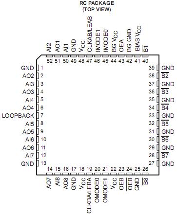 Specifications
Supply voltage range, VCC .............................................-0.5 V to 7V
Voltage range applied to any B output in the disabled
or power-off state,VO................................................-0.5 V to 3.5V
Voltage range applied to any output in the high state,
VO : A port..........................-0.5 V to VCC
Input voltage range, VI:Except B port ............................-1.2 V to 7V
B port .....................................-1.2 V to 3.5V
Input clamp current, IIK:Except B port .....................................-40mA
B port .................................................-18mA
Current applied to any single output in the low state, IO:
A port...................................................48mA
B port .................................................200mA
Package thermal impedance, JA(see Note 1):RC package...200/W
Storage temperature range, Tstg..................................-65 to 150
Description The SN74FB2033K is an 8-bit transceiver featuring a split input (AI) and output (AO) bus on the TTL-level A port. The common-I/O, open-collector B port operates at backplane transceiver logic (BTL) signal levels.
The logic element for data flow in each direction is configured by two mode inputs (IMODE1 and IMODE0 for B-to-A, OMODE1 and OMODE0 for A-to-B) as a buffer, a D-type flip-flop, or a D-type latch. When configured in the buffer mode, the inverted input data appears at the output port. In the flip-flop mode, data is stored on the rising edge of the appropriate clock input (CLKAB/LEAB or CLKBA/LEBA). In the SN74FB2033K latch mode, the clock inputs serve as active-high transparent latch enables.
Data flow in the B-to-A direction, regardless of the logic element selected, is further controlled by the LOOPBACK input. When SN74FB2033K LOOPBACK is low, B-port data is the B-to-A input. When LOOPBACK is high, the output of the selected A to-B logic element (prior to inversion) is the B-to-A input.
The SN74FB2033K AO port-enable/-disable control is provided by OEA. When OEA is low or when VCC is less than 2.5 V, the AO port is in the high-impedance state. When OEA is high, the AO port is active (high or low logic levels).
The SN74FB2033K B port is controlled by OEB and OEB. If OEB is low, OEB is high, or VCC is less than 2.5 V, the B port is inactive. If OEB is high and OEB is low, the B port is active.
BG VCC and BG GND are the bias-generator reference inputs.
The A-to-B and B-to-A logic elements are active, regardless of the state of their associated outputs. The logic elements can enter new data (in flip-flop and latch modes) or retain previously stored data while the associated outputs are in the high-impedance (AO port) or inactive (B port) states.
Output clamps are provided on the BTL outputs to reduce switching noise. One clamp reduces inductive ringing effects on VOH during a low-to-high transition. The other clamps out ringing below the BTL VOL voltage of 0.75 V. Both clamps are active only during ac switching and do not affect the BTL outputs during steady-state conditions.
BIAS VCC establishes a voltage between 1.62 V and 2.1 V on the BTL outputs when VCC is not connected. The SN74FB2033K is characterized for operation from 0°C to 70°C.

 SN74FB2033K Data Sheet


