Features: Bidirectional Interface Between GTL+Signal Levels and LVTTL Logic Levels
LVTTL Interfaces Are 5-V Tolerant
High-Drive GTL+ Outputs (100 mA)
LVTTL Outputs (-C24 mA/24 mA)
Variable Edge-Rate Control (ERC) Input Selects GTL+ Rise and Fall Times for Optimal Data-Transfer Rate and Signal Integrity
Ioff, Power-Up 3-State, and BIAS VCC Support Live Insertion
Polarity Control Selects True or Complementary Outputs
Package Options Include Plastic Small-Outline (D), Thin Very Small-Outline (DGV), and Thin Shrink Small-Outline(PW) Packages
Pinout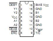 Specifications
Supply voltage range, VCC and BIAS VCC . . . . . . . . . . . . . . . . . . . -0.5 V to 4.6V
Input voltage range, VI (see Note 1):A and control inputs . . . . . . . . -0.5 V to 7V
B port, ERC, and VREF . . .. . . -0.5 V to 4.6V .
Voltage range applied to any output in the high-impedance or power-off state,VO
(see Note 1):Y . . . . . . . . . . . . . . . . . . . . . . . . . . . . . . . . . . . . . . . . . . -0.5 V to 7V
B port . . . . . . . . . . . . . . . . . . . . . .. . . . . . . . . . . . . . . . -0.5 V to 4.6V
Voltage range applied to any output in the high or low state, VO
(see Note 1):Y . . . . . . . . . . . . . . . . . . . . . . . . . . . . . . . . . -0.5 V to VCC + 0.5 V
B port . . . . . . . . . . . . . . . . . . . . . . . . . . . . . . . . . . .-0.5 V to 4.6V
Current into any output in the low state, IO :Y . . . . . . . . . . . . . . . . . . .48 mA
B port . . . . . . . . . . . . . . . .200 mA
Current into any output in the high state, IO(see Note 2) . . . . .. .. . . . .48 mA
Continuous current through each VCC or GND . . . . . . . . . . . . . . . . ..±100 mA
Input clamp current, IIK (VI < 0) . . . . . . . . . . . . . . . . . . . . . . . . . . . . ..-50 mA
Output clamp current, IOK (VO < 0) . . . . . . . . . . . . . . . . . . . . . . . . . . .-50 mA
(see Note 3):D package . . . . . . . . .73/W
Package thermal impedance, JA DGV package . . . . . . . . . . . . . . .120/W
PW package . . . . . . . . . . . . . . . .108/W
Storage temperature range, Tstg. . . . . . . . . . . . . . . . . . . . . . . .. . . .-65 to 150
DescriptionThe SN74GTLP1394 is a high-drive 2-bit 3-wire bus transceiver that provides LVTTL-to-GTL+ and GTL+-to-LVTTL signal-level translation. SN74GTLP1394 allows for transparent and inverted transparent modes of data transfer with separate LVTTL input and LVTTL output pins. The device provides a high-speed interface between cards operating at LVTTL logic levels and a backplane operating at GTL+ signal levels and is especially designed to work with the Texas Instruments TSB14C01A 1394 Backplane Physical-Layer Controller. High-speed (about two times faster than standard LVTTL or TTL) backplane operation is a direct result of GTLP!fls reduced output swing (<1 V), reduced input threshold levels, improved differential input, and outpu edge control (OECTM). Improved GTLP OEC circuits minimize bus settling time and have been designed and tested using several backplane models. The high drive is suitable for driving double-terminated low-impedance backplanes using incident-wave switching.
SN74GTLP1394 GTL+ is the Texas Instruments derivative of the Gunning transceiver logic (GTL) JEDEC standard JESD 8-3.The AC specification of the SN74GTLP1394 is given only at the preferred higher noise margin GTL+, but the user has the flexibility of using this device at either GTL (VTT = 1.2 V and VREF = 0.8 V) or GTL+ (VTT = 1.5 V and VREF= 1 V) signal levels.
Normally, the SN74GTLP1394 B port operates at GTL or GTL+ levels. The A inputs, Y outputs, and control inputs are compatible with LVTTL logic levels and are 5-V tolerant. VREF is the reference input voltage for the B port.
This SN74GTLP1394 device is fully specified for live-insertion applications using Ioff,power-up 3-state,and BIAS VCC.The Ioff circuitry disables the outputs, preventing damaging current backflow through the device when it is powered down. The power-up 3-state circuitry places the outputs in the high-impedance state during power up and power down, which prevents driver conflict. The BIAS VCC circuitry precharges and preconditions the B-port input/output connections, preventing disturbance of active data on the backplane during card insertion or removal, and permits true live-insertion capability.
SN74GTLP1394 High-drive GTLP backplane interface devices feature adjustable edge-rate control (ERC). Changing the ERC
input voltage between GND and V adjusts the B-port output rise and fall times. This allows the designer to
CC
optimize system data-transfer rate and signal integrity to the backplane load.
SN74GTLP1394 High-drive GTLP backplane interface devices feature adjustable edge-rate control (ERC). Changing the ERC input voltage between GND and VCC adjusts the B-port output rise and fall times. This allows the designer to optimize system data-transfer rate and signal integrity to the backplane load.

 SN74GTLP1394 Data Sheet


