SN74GTLP22034

Features: *Member of the Texas Instruments Widebus™ Family*TI-OPC™ Circuitry Limits Ringing on Unevenly Loaded Backplanes*OEC™ Circuitry Improves Signal Integrity and Reduces Electromagnetic Interference*Bidirectional Interface Between GTLP Signal Levels and LVTTL Logic L...

product image

SN74GTLP22034 Picture
SeekIC No. : 004498870 Detail

SN74GTLP22034: Features: *Member of the Texas Instruments Widebus™ Family*TI-OPC™ Circuitry Limits Ringing on Unevenly Loaded Backplanes*OEC™ Circuitry Improves Signal Integrity and Reduc...

floor Price/Ceiling Price

Part Number:
SN74GTLP22034
Supply Ability:
5000

Price Break

  • Qty
  • 1~5000
  • Unit Price
  • Negotiable
  • Processing time
  • 15 Days
Total Cost: $ 0.00

SeekIC Buyer Protection PLUS - newly updated for 2013!

  • Escrow Protection.
  • Guaranteed refunds.
  • Secure payments.
  • Learn more >>

Month Sales

268 Transactions

Rating

evaluate  (4.8 stars)

Upload time: 2025/12/24

Payment Methods

All payment methods are secure and covered by SeekIC Buyer Protection PLUS.

Notice: When you place an order, your payment is made to SeekIC and not to your seller. SeekIC only pays the seller after confirming you have received your order. We will also never share your payment details with your seller.
Product Details

Description


Features:

*Member of the Texas Instruments
  Widebus™ Family
*TI-OPC™ Circuitry Limits Ringing on
  Unevenly Loaded Backplanes
*OEC™ Circuitry Improves Signal Integrity
  and Reduces Electromagnetic Interference
*Bidirectional Interface Between GTLP
  Signal Levels and LVTTL Logic Levels
*Split LVTTL Port Provides a Feedback Path
  for Control and Diagnostics Monitoring
*AO Outputs Have Equivalent 26-Ω Series
  Resistors, So No External Resistors Are Required
*LVTTL Interfaces Are 5-V Tolerant
*High-Drive GTLP Open-Drain Outputs (100 mA)
*LVTTL Outputs (12 mA/12 mA)
*Variable Edge-Rate Control (ERC) Input Selects GTLP Rise and Fall Times for
  Optimal Data-Transfer Rate and Signal Integrity in Distributed Loads
*Ioff, Power-Up 3-State, and BIAS VCC
  Support Live Insertion
*Distributed VCC and GND Pins Minimize
  High-Speed Switching Noise
*Latch-Up Performance Exceeds 100 mA Per JESD 78, Class II
*ESD Protection Exceeds JESD 22
    2000-V Human-Body Model (A114-A)
    200-V Machine Model (A115-A)
    1000-V Charged-Device Model (C101)


Application

Audio
Automotive
Broadband
Digital Control
Military
Optical Networking
Security
Telephony
Video & Imaging
Wireless


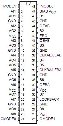
Pinout

  Connection Diagram


Specifications

Supply voltage range, VCC and BIAS VCC  . . . . . .  . . .  . . .  ..0.5 V to 4.6 V
Input voltage range, VI (see Note 1): AI port, ERC, and control inputs 
     . . . . . . .  . . .  . . .  . .  . . .  . . .  . . .  . .  . . .  . . .  . . .  . .  ..  .  0.5 V to 7 V
                                                            B port and VREF  .  . . .0.5 V to 4.6 V
Voltage range applied to any output in the high-impedance or power-off state
     VO(see Note 1): AO port  . . . . . . .  . . .  . . .  . . .  . .  . . . . . . 0.5 V to 7 V
B port  . . . . . . . . . . . .  . . .  . . .  . . .  . . .  . . .  . . .  . . .  .. . . . .0.5 V to 4.6 V
Current into any output in the low state, IO: AO port   . . .  . . .  .. . . . .24 mA
                                                                 B port   . . . . .  . . .  . . . . . .  100 mA
Current into any A-port output in the high state, IO (see Note 2)   . . . 24 mA
Continuous current through each VCC or GND  . . .  . . .  . . .  .  . . . . ±100 mA
Input clamp current, IIK (VI < 0)  . . . . . . . . . . . . . . . . . . . . . . . . . .  . . .-50mA
Output clamp current, IOK (VO < 0)  . . . . . . . .  . . . . . . . . . . . . . . . . .50 mA
Package thermal impedance, JA (see Note 3): DGG package . . . . . 70°C/W
                                                                           DGV package . . . . . 58°C/W
                                                                          GQL package . . . . . .42°C/W
Storage temperature range, Tstg   . . . . . . . . . . .. . .. .. . . . 65°C to 150°C


Description

      The SN74GTLP22034 is a high-drive, 8-bit, three-wire registered transceiver that provides true LVTTL-to-GTLP and GTLP-to-LVTTL signal-level translation. The device allows for transparent, latched, and flip-flop modes of data transfer with separate LVTTL input and LVTTL output pins, which provides a feedback path for control and diagnostics monitoring, the same functionality as the SN74FB2033, but with true logic. The device provides a high-speed interface between cards operating at LVTTL logic levels and a backplane operating at GTLP signal levels. High-speed (about three times faster than standard LVTTL or TTL) backplane operation is a direct result of GTLP's reduced output swing (<1 V), reduced input threshold levels, improved differential input, OEC™ circuitry, and TI-OPC circuitry. Improved GTLP OEC and TI-OPC circuits minimize bus-settling time and have been designed and tested using several backplane models. The high drive of the SN74GTLP22034 allows incident-wave switching in heavily loaded backplanes with equivalent load impedance down to 11 Ω.

      The AO outputs, which are designed to sink up to 12 mA, include equivalent 26-Ω resistors to reduce overshoot and undershoot.


Customers Who Bought This Item Also Bought

Margin,quality,low-cost products with low minimum orders. Secure your online payments with SeekIC Buyer Protection.
Cables, Wires
RF and RFID
Power Supplies - External/Internal (Off-Board)
Semiconductor Modules
Audio Products
View more