Features: ` Qualification in Accordance With AEC-Q100†
` Qualified for Automotive Applications
` Customer-Specific Configuration Control Can Be Supported Along With Major-Change Approval
` Targeted Specifically for High-Speed Memory Decoders and Data-Transmission Systems
` Wide Operating Voltage Range of 2 V to 6 V
` Outputs Can Drive up to Ten LSTTL Loads
` Low Power Consumption, 80-A Max ICC
` Typical tpd = 10 ns
` ±4-mA Output Drive at 5 V
` Low Input Current of 1 A Max
` Incorporate Two Enable Inputs to Simplify Cascading and/or Data Reception
` ESD Protection Level per AEC-Q100 Classification
− 2000-V (H2) Human-Body Model
− 200-V (M3) Machine Model
− 1000-V (C5) Charged-Device Model
† Contact factory for details. Q100 qualification data available on request.
Pinout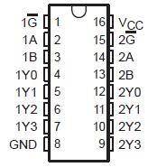 Specifications
Supply voltage range, VCC . . . . . . . . . . . . . . . . . . . . . . . . . . . . . . . . .. . . −0.5 V to 7 V
Input clamp current, IIK (VI < 0 or VI > VCC) (see Note 1) . . . . . . . . . . . .. . . . ±20 mA
Output clamp current, IOK (VO < 0 or VO > VCC) (see Note 1) . . . . . . . . .. . . . ±20 mA
Continuous output current, IO (VO = 0 to VCC) . . . . . . . . . . . . . . . . . . . . . . . . ±25 mA
Continuous current through VCC or GND . . . . . . . . . . . . . . . . . . . . . . . . . . . . . ±50 mA
Package thermal impedance, JA (see Note 2): D package . . . . . . . .. . . . . . . 73°C/W
PW package . . . . . . . . . . . . . . . . . . . . . . . . . . . . . . . . 108°C/W
Storage temperature range, Tstg . . . . . . . . . . . . . . . . . . . . . . . . . . . . −65°C to 150°C
† Stresses beyond those listed under "absolute maximum ratings" may cause permanent damage to the device. These are stress ratings only, and functional operation of the device at these or any other conditions beyond those indicated under "recommended operating conditions" is not implied. Exposure to absolute-maximum-rated conditions for extended periods may affect device reliability.
NOTES: 1. The input and output voltage ratings may be exceeded if the input and output current ratings are observed.
2. The package thermal impedance is calculated in accordance with JESD 51-7.
DescriptionThe SN74HC139Q1 device is designed for high-performance memory-decoding or data-routing applications requiring very short propagation delay times. In high-performance memory systems, this decoder can minimize the effects of system decoding. When employed with high-speed memories utilizing a fast enable circuit, the delay time of this decoder and the enable time of the memory usually are less than the typical access time of the memory. This means that the effective system delay introduced by the decoder is negligible.
The SN74HC139Q1 device comprises two individual 2-line to 4-line decoders in a single package. The active-low enable (G) input can be used as a data line in demultiplexing applications. This decoder/demultiplexer features fully buffered inputs, each of which represents only one normalized load to its driving circuit.

 SN74HC139Q1 Data Sheet


