Counter Type
:
Output Type
:
Maximum Operating Temperature
: + 85 C
Minimum Operating Temperature
: - 40 C
Number of Circuits
: 1
Logic Family
: 74HC
Counting Sequence
: Serial/Parallel to Serial
Logic Type
: CMOS
Number of Input Lines
: 9
Packaging
: Tube
Propagation Delay Time
: 150 ns, 30 ns, 26 ns
Package / Case
: PDIP-16
Features: ` Wide Operating Voltage Range of 2 V to 6 V
` Outputs Can Drive Up To 10 LSTTL Loads
` Low Power Consumption, 80-A Max ICC
` Typical tpd = 13 ns
` ±4-mA Output Drive at 5 V
` Low Input Current of 1 A Max
` Complementary Outputs
` Direct Overriding Load (Data) Inputs
` Gated Clock Inputs
` Parallel-to-Serial Data ConversionPinout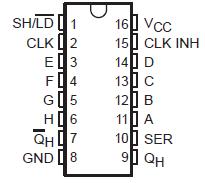 SpecificationsSupply voltage range, VCC . . . . . . . . . . . . . . . . . . . . . . . . . . . . . . . . . . . . . . . . . . . . . . . . . . . . . . . . . . −0.5 V to 7 V
Input clamp current, IIK (VI < 0 or VI > VCC) (see Note 1) . . . . . . . . . . . . . . . . . . . . . . . . . . . . . . . . . . . . ±20 mA
Output clamp current, IOK (VO < 0 or VO > VCC) (see Note 1) . . . . . . . . . . . . . . . . . . . . . . . . . . . . . . . . ±20 mA
Continuous output current, IO (VO = 0 to VCC) . . . . . . . . . . . . . . . . . . . . . . . . . . . . . . . . . . . . . . . . . . . . . . ±25 mA
Continuous current through VCC or GND . . . . . . . . . . . . . . . . . . . . . . . . . . . . . . . . . . . . . . . . . . . . . . . . . . . ±50 mA
Package thermal impedance, JA (see Note 2): D package . . . . . . . . . . . . . . . . . . . . . . . . . . . . . . . . . . . 73°C/W
DB package . . . . . . . . . . . . . . . . . . . . . . . . . . . . . . . . . 82°C/W
N package . . . . . . . . . . . . . . . . . . . . . . . . . . . . . . . . . . . 67°C/W
NS package . . . . . . . . . . . . . . . . . . . . . . . . . . . . . . . . . 64°C/W
PW package . . . . . . . . . . . . . . . . . . . . . . . . . . . . . . . . 108°C/W
Storage temperature range, Tstg . . . . . . . . . . . . . . . . . . . . . . . . . . . . . . . . . . . . . . . . . . . . . . . . . . . −65°C to 150°C
† Stresses beyond those listed under "absolute maximum ratings" may cause permanent damage to the device. These are stress ratings only, and functional operation of the device at these or any other conditions beyond those indicated under "recommended operating conditions" is not implied. Exposure to absolute-maximum-rated conditions for extended periods may affect device reliability.
NOTES: 1. The input and output voltage ratings may be exceeded if the input and output current ratings are observed.
2. The package thermal impedance is calculated in accordance with JESD 51-7.DescriptionThe SN74HC165N is designed as one kind of quadruple 2-input positive-or gates because of it contains four independent 2-input OR gates. Features of the SN74HC32N are:(1)low power consumption, 20-A max Icc;(2)outputs can drive up to 10 LSTTL loads;(3)wide operating voltage range of 2 V to 6 V;(4)typical tpd=8 ns;(5)±4-mA output drive at 5 V;(6)low input current of 1 A max.
The absolute maximum ratings of the SN74HC165N can be summarized as:(1)supply voltage range, Vcc:-0.5 V to 7 V;(2)input clamp current, IIK (VI < 0 or VI > Vcc):±20 mA;(3)output clamp current, IOK (VO < 0 or VO > Vcc):±20 mA;(4)continuous output current, IO (VO = 0 to Vcc):±25 mA;(5)continuous current through Vcc or GND:±50 mA;(6)package thermal impedance:80°C/W;(7)storage temperature range:-65°C to 150°C.
Texas Instruments Incorporated and its subsidiaries (TI) reserve the right to make corrections, modifications, enhancements, improvements, and other changes to its products and services at any time and to discontinue any product or service without notice. Customers should obtain the latest relevant information before placing orders and should verify that such information is current and complete. All products are sold subject to TI's terms and conditions of sale supplied at the time of order acknowledgment. If you want to know more information such as the electrical characteristics about the SN74HC165N, please download the datasheet in www.seekic.com or www.chinaicmart.com.

 SN74HC165N Data Sheet


