Features: · Eight D-Type Flip-Flops in a Single Package
· High-Current 3-State True Outputs Can Drive up to 15 LSTTL Loads
· Full Parallel Access for Loading
· Package Options Include Plastic Shrink Small-Outline (DB), Small-Outline (DW), Thin Shrink Small-Outline (PW), and Ceramic Flat (W) Packages, Ceramic Chip Carriers (FK), and Standard Plastic (N) and Ceramic (J) DIPs
Pinout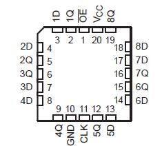 Specifications
Supply voltage range, VCC . . . . . . . . . . . . . . . . . . . . . . . . . . . . . . . . . . . . . . . . . . . . . . .0.5 V to 7 V
Input clamp current, IIK (VI < 0 or VI > VCC) (see Note 1) . . . . . . . . . . . . . . . . . . . . . . . . . . . ±20 mA
Output clamp current, IOK (VO < 0 or VO > VCC) (see Note 1) . . . . . . . . . . . . . . . .. . . . . . . . . ±20 mA
Continuous output current, IO (VO = 0 to VCC) . . . . . . . . . . . . . . . . . . . . . . . . . . . . . . . . . . . . ±35 mA
Continuous current through VCC or GND . . . . . . . . . . . . . . . . . . . . . . . . . . . . . . . . . . . . . . . . . ±70 mA
Package thermal impedance, JA (see Note 2): DB package . . . . . . . . . . . . . . . . . . . . . . . . 115°C/W
DW package . . . . . . . . . . . . . . . . . . . . . . . . 97°C/W
N package . . . . . . . . . . . . . . . . . . . . . . . . . . . 67°C/W
PW package . . . . . . . . . . . . . . . . . . . . . . . . 128°C/W
Storage temperature range, Tstg . . . . . . . . . . . . . . . . . . . . . . . . . . . . . . . . . . . .. . . . 65°C to 150°C
‡ Stresses beyond those listed under "absolute maximum ratings" may cause permanent damage to the device. These are stress ratings only, and functional operation of the device at these or any other conditions beyond those indicated under "recommended operating conditions" is not implied. Exposure to absolute-maximum-rated conditions for extended periods may affect device reliability.
NOTES: 1. The input and output voltage ratings may be exceeded if the input and output current ratings are observed.
2. The package thermal impedance is calculated in accordance with JESD 51, except for through-hole packages, which use a trace length of zero.
DescriptionThese 8-bit flip-flops feature 3-state outputs designed specifically for driving highly capacitive or relatively low-impedance loads. SN74HC374 are particularly suitable for implementing buffer registers, I/O ports, bidirectional bus drivers, and working registers.
The eight flip-flops of the 'HC374 devices SN74HC374 are edge-triggered D-type flip-flops. On the positive transition of the clock (CLK) input, the Q outputs are set to the logic levels that were set up at the data (D) inputs.
An output-enable (OE) input places the eight outputs in either a normal logic state (high or low logic levels) or the high-impedance state. In the high-impedance state, the SN74HC374 outputs neither load nor drive the bus lines significantly. The high-impedance state and increased drive provide the capability to drive bus lines without interface or pullup components.
OE does not affect the internal operations of the SN74HC374 flip-flops. Old data can be retained or new data can be entered while the outputs are in the high-impedance state.
To ensure the high-impedance state during power up or power down, OE should be tied to VCC through a pullup resistor; the minimum value of the resistor SN74HC374 is determined by the current-sinking capability of the driver.
The SN54HC374 is characterized for operation over the full military temperature range of 55°C to 125°C. The SN74HC374 is characterized for operation from 40°C to 85°C.

 SN74HC374 Data Sheet


