SN74HC4852

Features: Injection Current Cross−Coupling <1mV/mA (see Figure 1) Low Crosstalk Between Switches Pin Compatible with SN74HC4052,SN74LV4052A, and CD4052B 2-V to 6-V VCC Operation Latch-Up Performance Exceeds 100 mA Per JESD 78, Class II ESD Protection Exceeds JESD 22ApplicationAudiowww.ti...

product image

SN74HC4852 Picture
SeekIC No. : 004498951 Detail

SN74HC4852: Features: Injection Current Cross−Coupling <1mV/mA (see Figure 1) Low Crosstalk Between Switches Pin Compatible with SN74HC4052,SN74LV4052A, and CD4052B 2-V to 6-V VCC Operation Latch-Up P...

floor Price/Ceiling Price

Part Number:
SN74HC4852
Supply Ability:
5000

Price Break

  • Qty
  • 1~5000
  • Unit Price
  • Negotiable
  • Processing time
  • 15 Days
Total Cost: $ 0.00

SeekIC Buyer Protection PLUS - newly updated for 2013!

  • Escrow Protection.
  • Guaranteed refunds.
  • Secure payments.
  • Learn more >>

Month Sales

268 Transactions

Rating

evaluate  (4.8 stars)

Upload time: 2025/12/24

Payment Methods

All payment methods are secure and covered by SeekIC Buyer Protection PLUS.

Notice: When you place an order, your payment is made to SeekIC and not to your seller. SeekIC only pays the seller after confirming you have received your order. We will also never share your payment details with your seller.
Product Details

Description


Features:

Injection Current Cross−Coupling <1mV/mA (see Figure 1)
Low Crosstalk Between Switches
Pin Compatible with SN74HC4052,SN74LV4052A, and CD4052B
2-V to 6-V VCC Operation
Latch-Up Performance Exceeds 100 mA Per JESD 78, Class II
ESD Protection Exceeds JESD 22


Application

Audio                                www.ti.com/audio
Automotive                       www.ti.com/automotive
Broadband                        www.ti.com/broadband
Digital Control                   www.ti.com/digitalcontrol
Military                              www.ti.com/military
Optical Networking           www.ti.com/opticalnetwork
Security                            www.ti.com/security
Telephony                        www.ti.com/telephony
Video & Imaging               www.ti.com/video
Wireless                           www.ti.com/wireless


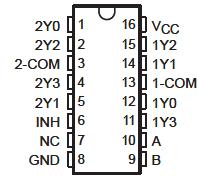
Pinout

  Connection Diagram


Specifications

Supply voltage range, VCC . . . . . . . . . . . . . . . . . . . . . . .. . . . . . . . . . . . . . . . . . . . . −0.5 V to 4.6 V
Input voltage range, VI (see Note 1) . . . . . . . . . . . . . . . . .  . . . . . . . . . . . . . . .. . . . . −0.5 V to 7 V
Switch I/O voltage range, VIO (see Notes 1 and 2). . . . . . . . . . . . . . . . . . . . −0.5 V to VCC + 0.5 V
Input clamp current, IIK (VI < 0 or VI > VCC) .  . . . . . . . . . . . . . . . . . . . . . . . . . . . . . . . . . . ±20 mA
I/O diode current, IIOK (VIO < 0 or VIO > VCC) . . . . . . . . . . . . . . . . . . . . . . . . . . . . . . . .. . . ±20 mA
Switch through current, IS (VIO = 0 to VCC) . . . . . . . . . . . . . . . . . . . . . . . . . . . . . . . . . . . . . ±25 mA
Continuous current through VCC or GND . . . . . . . . . . . . . . . . . . .. . . . . . ... . . . . . . . . . . . . . ±50 mA

Package thermal impedance, JA (see Note 3): DB package  . . . . . . . . . . . . . . . . . . . . . . . . 63°C/W
                                                                          DGV package  . . . . . . . . . . . . . . . . . . . . . . . 86°C/W
                                                                          NS package. . . . . . . . . . . . . . . . . . . . . . . . . . 65°C/W
                                                                          PW package . . . . . . . . . . . . . . . . . . . . . . . . . 88°C/W
Storage temperature range, Tstg . . . . . . . . . . . . . . . . . . . . . . . . . . . . . . . . . . . . . . . −65°C to 150°C
† Stresses beyond those listed under "absolute maximum ratings" may cause permanent damage to the device. These are stress ratings only, and functional operation of the device at these or any other conditions beyond those indicated under "recommended operating conditions" is not implied. Exposure to absolute-maximum-rated conditions for extended periods may affect device reliability.
NOTES: 1. The input and output voltage ratings may be exceeded if the input and output current ratings are observed.
             2. This value is limited to 5.5 V maximum.
             3. The package thermal impedance is calculated in accordance with JESD 51-7.


Description

This dual 4-to-1 CMOS analog multiplexer/demultiplexer SN74HC4852 is pin compatible with the 4052 function and also features injection-current effect control. This feature has excellent value in automotive applications where voltages in excess of normal supply voltages are common.

The injection-current effect control allows signals at disabled analog input channels to exceed the supply voltage without affecting the signal of the enabled analog channel. SN74HC4852 eliminates the need for external diode/resistor networks typically used to keep the analog channel signals within the supply voltage range.


Customers Who Bought This Item Also Bought

Margin,quality,low-cost products with low minimum orders. Secure your online payments with SeekIC Buyer Protection.
Discrete Semiconductor Products
Optoelectronics
Hardware, Fasteners, Accessories
Circuit Protection
Industrial Controls, Meters
Memory Cards, Modules
View more