Features: · Inputs Are TTL-Voltage Compatible
· Designed Specifically for High-Speed Memory Decoders and Data Transmission Systems
· Incorporate Two Enable Inputs to Simplify Cascading and/or Data Reception
· Package Options Include Plastic Small-Outline (D), Shrink Small-Outline (DB), Thin Shrink Small-Outline (PW), and Ceramic Flat (W) Packages, Ceramic Chip Carriers (FK), and Standard Plastic (N) and Ceramic (J) 300-mil DIPs
Pinout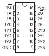 Specifications
Supply voltage range, VCC . . . . . . . . . . . . . . . . . . . . . . . . . . . . . . . . . . . . . . . . . . 0.5 V to 7 V
Input clamp current, IIK (VI < 0 or VI > VCC) (see Note 1) . . . . . . . . . . . . . . . . . . . . . . ±20 mA
Output clamp current, IOK (VO < 0 or VO > VCC) (see Note 1) . . . . . . . . . . . . . . . . . . . . ±20 mA
Continuous output current, IO (VO = 0 to VCC) . . . . . . . . . . . . . . . . . . . . . . . .. . . . . . . . ±25 mA
Continuous current through VCC or GND . . . . . . . . . . . . . . . . . . . . . . . . . . . . . . .. . . . . . ±50 mA
Package thermal impedance, JA (see Note 2): D package . . . . . . . . . . . . . . . . . . . .. 113°C/W
DB package . . . . . . . . . . . . . . . . . . . . 131°C/W
N package . . . . . . . . . . . . . . . . .. . . . . . 78°C/W
PW package . . . . . . . . . . . . . . . . . . . . 149°C/W
Storage temperature range, Tstg . . . . . . . . . . . . . . . . . . . . . . . . . . . . . . . .. . . 65°C to 150°C
† Stresses beyond those listed under "absolute maximum ratings" may cause permanent damage to the device. These are stress ratings only, and functional operation of the device at these or any other conditions beyond those indicated under "recommended operating conditions" is not implied. Exposure to absolute-maximum-rated conditions for extended periods may affect device reliability.
NOTES: 1. The input and output voltage ratings may be exceeded if the input and output current ratings are observed.
2. The package thermal impedance is calculated in accordance with JESD 51, except for through-hole packages, which use a trace length of zero.
DescriptionThe SN74HCT139 are designed for high-performance memory-decoding or data-routing applications requiring very short propagation delay times. In high-performance memory systems, these decoders can minimize the effects of system decoding. When employed with high-speed memories utilizing a fast enable circuit, the delay time of these decoders and the enable time of the memory are usually less than the typical access time of the memory. This means that the effective system delay introduced by the decoders is negligible.
The SN74HCT139 comprise two individual 2-line to 4-line decoders in a single package. The active-low enable (G) input can be used as a data line in demultiplexing applications. These decoders/demultiplexers feature fully buffered inputs, each of which represents only one normalized load to its driving circuit.
The SN74HCT139 is characterized for operation over the full military temperature range of 55°C to 125°C. The SN74HCT139 is characterized for operation from 40°C to 85°C.

 SN74HCT139 Data Sheet


