SN74HSTL162822

Features: · Member of the Texas Instruments WidebusE Family· Inputs Meet JEDEC HSTL Standard JESD8-6· All Outputs Have Equivalent 25-W Series Resistors· Packaged in Plastic Thin Shrink Small-Outline PackagePinoutSpecificationsSupply voltage range, VCC . . . . . . . . . . . . . . . . . . . . . . . ...

product image

SN74HSTL162822 Picture
SeekIC No. : 004499002 Detail

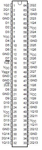
SN74HSTL162822: Features: · Member of the Texas Instruments WidebusE Family· Inputs Meet JEDEC HSTL Standard JESD8-6· All Outputs Have Equivalent 25-W Series Resistors· Packaged in Plastic Thin Shrink Small-Outline...

floor Price/Ceiling Price

Part Number:
SN74HSTL162822
Supply Ability:
5000

Price Break

  • Qty
  • 1~5000
  • Unit Price
  • Negotiable
  • Processing time
  • 15 Days
Total Cost: $ 0.00

SeekIC Buyer Protection PLUS - newly updated for 2013!

  • Escrow Protection.
  • Guaranteed refunds.
  • Secure payments.
  • Learn more >>

Month Sales

268 Transactions

Rating

evaluate  (4.8 stars)

Upload time: 2025/12/24

Payment Methods

All payment methods are secure and covered by SeekIC Buyer Protection PLUS.

Notice: When you place an order, your payment is made to SeekIC and not to your seller. SeekIC only pays the seller after confirming you have received your order. We will also never share your payment details with your seller.
Product Details

Description


Features:

· Member of the Texas Instruments WidebusE Family
· Inputs Meet JEDEC HSTL Standard JESD8-6
· All Outputs Have Equivalent 25-W Series Resistors
· Packaged in Plastic Thin Shrink Small-Outline Package


Pinout

  Connection Diagram


Specifications

Supply voltage range, VCC . . . . . . . . . . . . . . . . . . . . . . . . . . . . . . . . . . . . . . . . . . 0.5 V to 4.6 V
Input voltage range, VI (see Note 1) . . . . . . . . . . . . . . . . . . . . . . . . . . . . . 0.5 V to VCC + 0.5 V
Output voltage range, VO (see Note 1) . . . . . . . . . . . . . . . . . . . . . . . . . . .  0.5 V to VCC + 0.5 V
Input clamp current, IIK (VI < 0) . . . . . . . . . . . . . . . . . . . . . . . . . . . . . . . . . . . . . . . . . . . .50 mA
Output clamp current, IOK (VO < 0 or VO > VCC) (see Note 2) . . . . . . . . . . . . . . . . . . . .  ±50 mA
Continuous output current, IO (VO = 0 to VCC) . . . . . . . . . . . . . . . . . . . . . . . . . . . . . . . . ±50 mA
Continuous current through each VCC or GND . . . . . . . . . . . . . . . . . . . . . . . . . . . . . . . .  ±100 mA
Package thermal impedance, JA (see Note 3) . . . . . . . . . . . . . . . . . . . . . . . . . . . . . . . . . .74/W
Storage temperature range, Tstg . . . . . . . . . . . . . . . . . . . . . . . . . . . . . . . . . . . . . .65 to 150


Description

This 14-bit to 28-bit D-type latch is designed for 3.15-V to 3.45-V VCC operation. HSTL levels are expected on the inputs. LVTTL levels are driven on the Q outputs.

All outputs are designed to sink up to 12 mA and include 25-W series resistors to reduce overshoot and undershoot.

The SN74HSTL162822 is particularly suitable for driving an address bus to two banks of memory. Each bank of 14 outputs is controlled with its own latch-enable (LE) input.

Each of the 14 data (D) inputs is tied to the inputs of two D-type latches, which provide true data at the outputs. While LE is low, the outputs (Q) of the corresponding 14 latches follow the D inputs. When LE is taken high, the Q outputs are latched at the levels set up at the D inputs.

The SN74HSTL162822 is characterized for operation from 40°C to 90°C.


Customers Who Bought This Item Also Bought

Margin,quality,low-cost products with low minimum orders. Secure your online payments with SeekIC Buyer Protection.
Potentiometers, Variable Resistors
Boxes, Enclosures, Racks
Cable Assemblies
LED Products
Optical Inspection Equipment
Static Control, ESD, Clean Room Products
View more