SN74LS195A

PinoutDescriptionThe LS195A Logic Diagram and Truth Table indicate the functionalcharacteristics of the LS195A 4-Bit Shift Register. The deviceis useful in a wide variety of shifting, counting and storageapplications. It performs serial, parallel, serial to parallel, orparallel to serial data tran...

product image

SN74LS195A Picture
SeekIC No. : 004499031 Detail

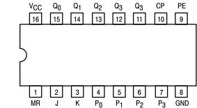
SN74LS195A: PinoutDescriptionThe LS195A Logic Diagram and Truth Table indicate the functionalcharacteristics of the LS195A 4-Bit Shift Register. The deviceis useful in a wide variety of shifting, counting and s...

floor Price/Ceiling Price

Part Number:
SN74LS195A
Supply Ability:
5000

Price Break

  • Qty
  • 1~5000
  • Unit Price
  • Negotiable
  • Processing time
  • 15 Days
Total Cost: $ 0.00

SeekIC Buyer Protection PLUS - newly updated for 2013!

  • Escrow Protection.
  • Guaranteed refunds.
  • Secure payments.
  • Learn more >>

Month Sales

268 Transactions

Rating

evaluate  (4.8 stars)

Upload time: 2025/12/24

Payment Methods

All payment methods are secure and covered by SeekIC Buyer Protection PLUS.

Notice: When you place an order, your payment is made to SeekIC and not to your seller. SeekIC only pays the seller after confirming you have received your order. We will also never share your payment details with your seller.
Product Details

Description


Pinout

  Connection Diagram


Description

The LS195A Logic Diagram and Truth Table indicate the functionalcharacteristics of the LS195A 4-Bit Shift Register. The deviceis useful in a wide variety of shifting, counting and storageapplications. It performs serial, parallel, serial to parallel, orparallel to serial data transfers at very high speeds.

The LS195A has two primary modes of operation, shift right(Q0  º  Q1) and parallel load which are controlled by the state ofthe Parallel Enable (PE) input. When the PE input is HIGH,serial data enters the first flip-flop Q0 via the J and K inputs andis shifted one bit in the direction Q0  º  Q1  º  Q2  º  Q3 followingeach LOW to HIGH clock transition. The JK inputs provide theflexibility of the JK type input for special applications, and thesimple D type input forgeneral applications by tying the twopins together. When the PE input is LOW, the LS195A appearsas four common clocked D flip-flops. The data on the parallelinputs P0, P1, P2, P3 is transferred to the respective Q0, Q1,Q2, Q3 outputs following the LOW to HIGH clock transition.

LS195A Shift left operations (Q3  º  Q2) can be achieved by tying the QnOutputs to the Pn1 inputs and holding the PE input LOW.All serial and parallel datatransfers are synchronous,occurring after each LOW to HIGH clock transition. Since theLS195A utilizes edge-triggering, there is no restriction on theactivity of the J, K, Pn and PE inputs for logic operation -except for the set-up and release time requirements.

LS195A A LOW on the asynchronous Master Reset (MR) input setsall Q outputs LOW, independent of any other input condition.


Customers Who Bought This Item Also Bought

Margin,quality,low-cost products with low minimum orders. Secure your online payments with SeekIC Buyer Protection.
Resistors
Crystals and Oscillators
Discrete Semiconductor Products
Connectors, Interconnects
Programmers, Development Systems
View more