SN74LS224A

Features: · Independent Synchronous Inputs and utputs· 16 Words by 4 Bits Each· 3-State Outputs Drive Bus Lines Directly· Data Rates up to 10 MHz· Fall-Through Time 50 ns Typical· Data Terminals Arranged for Printed Circuit ard Layout· Expandable Using External Gating· Packaged in Standard...

product image

SN74LS224A Picture
SeekIC No. : 004499038 Detail

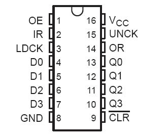
SN74LS224A: Features: · Independent Synchronous Inputs and utputs· 16 Words by 4 Bits Each· 3-State Outputs Drive Bus Lines Directly· Data Rates up to 10 MHz· Fall-Through Time 50 ns Typical· Data Termina...

floor Price/Ceiling Price

Part Number:
SN74LS224A
Supply Ability:
5000

Price Break

  • Qty
  • 1~5000
  • Unit Price
  • Negotiable
  • Processing time
  • 15 Days
Total Cost: $ 0.00

SeekIC Buyer Protection PLUS - newly updated for 2013!

  • Escrow Protection.
  • Guaranteed refunds.
  • Secure payments.
  • Learn more >>

Month Sales

268 Transactions

Rating

evaluate  (4.8 stars)

Upload time: 2025/12/24

Payment Methods

All payment methods are secure and covered by SeekIC Buyer Protection PLUS.

Notice: When you place an order, your payment is made to SeekIC and not to your seller. SeekIC only pays the seller after confirming you have received your order. We will also never share your payment details with your seller.
Product Details

Description


Features:

· Independent Synchronous Inputs and utputs
· 16 Words by 4 Bits Each
· 3-State Outputs Drive Bus Lines Directly
· Data Rates up to 10 MHz
· Fall-Through Time 50 ns Typical
· Data Terminals Arranged for Printed Circuit
  ard Layout
· Expandable Using External Gating
· Packaged in Standard Plastic 300-mil DIPs


Pinout

  Connection Diagram


Specifications

Supply voltage range, VCC (see Note 1) . . . . . . . . . . . . . . . . . . . . . . . . . . . . . . . . . . . . . . . . . . . . . 0.5 V to 7 V
Input voltage range, VI . . . . . . . . . . . . . . . . . . . . . . . . . . . . . . . . . . . . . . . . . . . . . . . . . . . . . . . . . .  0.5 V to 7 V
Off-state output voltage range, VO . . . . . . . . . . . . . . . . . . . . . . . . . . . . . . . . . . . . . . . . . . . . . . . . 0.5 V to 5.5 V
Package thermal impedance, qJA (see Note 2) . . . . . . . . . . . . . . . . . . . . . . . . . . . . . . . . . . . . . . . . . . . . . 78°C/W
Storage temperature range, Tstg . . . . . . . . . . . . . . . . . . . . . . . . . . . . . . . . . . . . . . . . . . . . . . . . .65°C to 150°C
† Stresses beyond those listed under "absolute maximum ratings" may cause permanent damage to the device. These are stress ratings only and
functional operation of the device at these or any other conditions beyond those indicated under "recommended operating conditions" is not
implied. Exposure to absolute-maximum-rated conditions for extended periods may affect device reliability.
NOTES: 1. All voltage values are with respect to GND.
2. The package thermal impedance is calculated in accordance with JESD 51.


Description

The SN74LS224A 64-bit, low-power Schottky memory is organized as 16 words by 4 bits each. It can be expanded in multiples of 15m + 1 words or 4n bits, or both (where n is the number of packages in the vertical array and m is the number of packages in the horizontal array); however, some external gating is required. For longer words, the input ready (IR) signals of the first-rank packages and output ready (OR) signals of the last-rank packages must be ANDed for proper synchronization.

A first-in, first-out (FIFO) memory is a storage device that allows data to be written to and read from its array at independent data rates. These FIFOs are designed to process data at rates up to 10 MHz in a bit-parallel format, word by word.

The load clock (LDCK) normally is held low, and data is written into memory on the high-to-low transition of LDCK. The unload clock (UNCK) normally is held high, and data is read out on the low-to-high transition of UNCK. The memory is full when the number of words clocked in exceeds by 16 the number of words clocked out. When the memory is full, LDCK signals have no effect on the data residing in memory. When the memory is empty, UNCK signals have no effect.

Status of the FIFO memory is monitored by the IR and OR flags that indicate not-full and not-empty conditions. IR is high only when the memory is not full and LDCK is low. OR is high only when the memory is not empty and UNCK is high.

A low level on the clear (CLR) input resets the internal stack-control pointers and also sets IR high and OR low to indicate that old data remaining at the data outputs is invalid. Data outputs are noninverting with respect to the data inputs and are at high impedance when the output-enable (OE) input is low. OE does not affect the IR and OR outputs.

The SN74LS224A is characterized for operation from 0°C to 70°C.


Customers Who Bought This Item Also Bought

Margin,quality,low-cost products with low minimum orders. Secure your online payments with SeekIC Buyer Protection.
Cables, Wires - Management
Crystals and Oscillators
Circuit Protection
Discrete Semiconductor Products
Optoelectronics
Potentiometers, Variable Resistors
View more