Features: *Choice of Eight Latches or Eight D-Type
Flip-Flops in a Single Package
*3-State Bus-Driving Outputs
*Full Parallel Access for Loading
*Buffered Control Inputs
*Clock-Enable Input Has Hysteresis to
Improve Noise Rejection ('S373 and 'S37)
*P-N-P Inputs Reduce DC Loading on Data
Lines ('S373 and 'S37)ApplicationAudio
Automotive
Broadband
Digital Control
Military
Optical Networking
Security
Telephony
Video & Imaging
WirelessPinout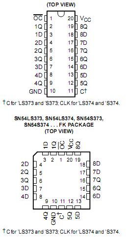 SpecificationsSupply voltage, VCC (see Note 1). . . . . . . . . . . . . . . . . . . . . . . . . . . . . . . . . . . . . . . . . . . . . . . . . . . . . . . . . 7 V
Input voltage, VI. . . . . . . . . . . . . . . . . . . . . . . . . . . . . . . . . . . . . . . . . . . . . . . . . . . . . . . . . . . . . . . ..............7 V
Off-state output voltage . . . . . . . . . . . . . . . . . . . . . . . . . . . . . . . . . . . . . . . . . . . . . . . . . . . . . . . . . . . . . . .5.5 V
Package thermal impedance, JA (see Note 2):DB package ...................................................................70°C/W
DW package ...................................................................58°C/W
N package .......................................................................59°C/W
NS package .....................................................................60°C/W
Storage temperature range, Tstg..............................................................................................65°C to 150°C
DescriptionThese 'LS373 and 'S373 8-bit registers feature 3-state outputs designed specifically for driving highly capacitive or relatively low-impedance loads. The high-impedance 3-state and increased high-logic-level drive provide these registers with the capability of being connected directly to and driving the bus lines in a bus-organized system without need for interface or pullup components. These devices are particularly attractive for implementing buffer registers, I/O ports, bidirectional bus drivers, and working registers.
The eight latches of the 'LS373 and 'S373 are transparent D-type latches, meaning that while the enable (C or CLK) input is high, the Q outputs follow the data (D) inputs. When C or CLK is taken low, the output is latched at the level of the data that was set up.
The eight flip-flops of the 'LS374 and 'S374 are edge-triggered D-type flip-flops. On the positive transition of the clock, the Q outputs are set to the logic states that were set up at the D inputs.
Schmitt-trigger buffered inputs at the enable/clock lines of the 'S373 and 'S374 devices simplify system design as ac and dc noise rejection is improved by typically 400 mV due to the input hysteresis. A buffered output-control (OC</a>) input can be used to place the eight outputs in either a normal logic state (high or low logic levels) or the high-impedance state. In the high-impedance state, the outputs neither load nor drive the bus lines significantly.
OC</a> does not affect the internal operation of the latches or flip-flops. That is, the old data can be retained or new data can be entered, even while the outputs are off.

 SN74LS373 Data Sheet


