SN74LV139A

PinoutSpecificationsSupply voltage range, VCC . . . . . . . . . . . . . . . . . . . . . . . . . . . .. . . . . . 0.5 V to 7 VInput voltage range, VI (see Note 1) . . . . . . . . . . . . . . . . . . . . . .. . . . 0.5 V to 7 VVoltage range applied to any output in the high-impedance or power-off st...

product image

SN74LV139A Picture
SeekIC No. : 004499135 Detail

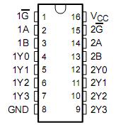
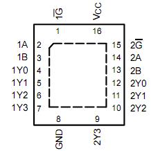
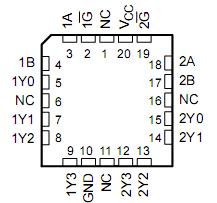
SN74LV139A: PinoutSpecificationsSupply voltage range, VCC . . . . . . . . . . . . . . . . . . . . . . . . . . . .. . . . . . 0.5 V to 7 VInput voltage range, VI (see Note 1) . . . . . . . . . . . . . . . . . . ...

floor Price/Ceiling Price

Part Number:
SN74LV139A
Supply Ability:
5000

Price Break

  • Qty
  • 1~5000
  • Unit Price
  • Negotiable
  • Processing time
  • 15 Days
Total Cost: $ 0.00

SeekIC Buyer Protection PLUS - newly updated for 2013!

  • Escrow Protection.
  • Guaranteed refunds.
  • Secure payments.
  • Learn more >>

Month Sales

268 Transactions

Rating

evaluate  (4.8 stars)

Upload time: 2025/12/30

Payment Methods

All payment methods are secure and covered by SeekIC Buyer Protection PLUS.

Notice: When you place an order, your payment is made to SeekIC and not to your seller. SeekIC only pays the seller after confirming you have received your order. We will also never share your payment details with your seller.
Product Details

Description


Pinout

  Connection Diagram  Connection Diagram  Connection Diagram


Specifications

Supply voltage range, VCC . . . . . . . . . . . . . . . . . . . . . . . . . . . .. . . . . . 0.5 V to 7 V
Input voltage range, VI (see Note 1) . . . . . . . . . . . . . . . . . . . . . .. . . . 0.5 V to 7 V
Voltage range applied to any output in the high-impedance
    or power-off state, VO (see Note 1) . . . . . . . . . . . . . . . . . . . .. . . . . 0.5 V to 7 V
Output voltage range, VO (see Notes 1 and 2) . . . . . . . . .. . . 0.5 V to VCC + 0.5 V
Input clamp current, IIK (VI < 0) . . . . . . . . . . . . . . . . . . . . . .. . . . . . . . . . . . 20 mA
Output clamp current, IOK (VO < 0 or VO > VCC) . . . . . . . . . . . . . .  . . . . . . . ±50 mA
Continuous output current, IO (VO = 0 to VCC) . . . . . . . . . . . . . . .  . . . . . . . ±25 mA
Continuous current through VCC or GND . . . . . . . . . . . . . . . . . . . . .  . . . . . . ±50 mA
Package thermal impedance, JA  (see Note 3): D package . . . . . . . .  . . . . 73°C/W
                                                     (see Note 3): DB package . . . . . . . .. . . . 82°C/W
                                                     (see Note 3): DGV package . . . . ... . . . 120°C/W
                                                     (see Note 3): NS package . . . . . . . . . . . 64°C/W
                                                     (Note 3): PW package . . . . . . . . . . . . . 108°C/W
                                                     (see Note 4): RGY package . . . . . . . . . . 39°C/W
Storage temperature range, Tstg . . . . . . . . . . . . . . . . . . . . . . . . 65°C to 150°C


Description

The 'LV139A devices are dual 2-line to 4-line decoders/demultiplexers designed for 2-V to 5.5-V VCC operation.

These devices LV139A are designed for high-performance memory-decoding or data-routing applications requiring very short propagation delay times. In high-performance memory systems, these decoders can minimize the effects of system decoding. When employed with high-speed memories utilizing a fast enable circuit, the delay time of these decoders and the enable time of the memory usually are less than the typical access time of the memory. This means that the effective system delay introduced by the decoders is negligible.

The 'LV139A devices comprise two individual 2-line to 4-line decoders in a single package. The active-low enable (G ) input can be used as a data line in demultiplexing applications. These decoders/demultiplexers feature fully buffered inputs, each of which represents only one normalized load to its driving circuit.

These devices LV139A are fully specified for partial-power-down applications using Ioff. The Ioff circuitry disables the outputs, preventing damaging current backflow through the devices when they are powered down.


Customers Who Bought This Item Also Bought

Margin,quality,low-cost products with low minimum orders. Secure your online payments with SeekIC Buyer Protection.
Crystals and Oscillators
Static Control, ESD, Clean Room Products
Test Equipment
RF and RFID
Undefined Category
Optical Inspection Equipment
View more