Features: EPICTM(Enhanced-Performance ImplantedCMOS) Process
High On-Off Output-Voltage Ratio
Low Crosstalk Between Switches
Individual Switch Controls
Extremely Low Input Current
ESD Protection Exceeds 2000 V PerMIL-STD-883, Method 3015; Exceeds 200 VUsing Machine Model (C = 200 pF, R = 0)
Package Options Include PlasticSmall-Outline (D, NS), Shrink Small-Outline(DB), Thin Very Small-Outline (DGV), ThinShrink Small-Outline (PW), Ceramic Flat(W) Packages, and Standard Plastic (N) andCeramic (J) DIPs
Pinout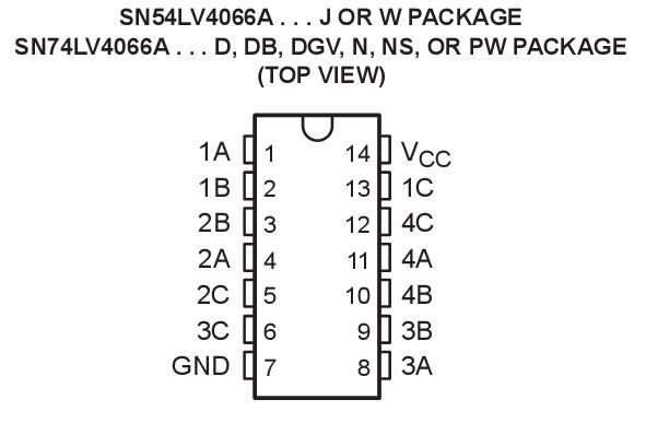 Specifications
Supply voltage range, VCC(see Note 1) . . . . . . . . . . . . . . . . . . . . . . . . . . . . . . . . . 0.5 V to 7 V
Input voltage range, VI(see Note 1) . . . . . . . . . . . . . . . .. . . . . . . . . . . . . . . . . . . . 0.5 V to 7 V
Switch I/O voltage range, VIO(see Note 1 and 2) . . . . . . . . . . . . . . . . . . . . 0.5 V to VCC+ 0.5 V
Control-input clamp current, IIK(VI< 0) . . . . . . . . . . . . . . . . . . . . . . . . . . . . . . . . . . . . . . . 20 mA
I/O diode current, IIOK (VIO< 0 or VIO > VCC) . . . . . . . . . . . . . . . . . . . . . . . . . . . . . . . . . ±50 mA
On-state switch current, IT (VIO = 0 to VCC) . . . . . . . . . . . . . . . . . . . . . . . . . . . . . . . . . . . ±25 mA
Continuous current through VCC or GND . . . . . . . . . . . . .. . . . . . . . . . . . . . . . . . . . . . . . . .±50 mA
Package thermal impedance, JA (see Note 3): D package . . . . . . . . . . . . . . . . . . . . . . . . . 127/W
DB package . . . . . . . . . . . . . . . . . . . . . . . . 158/W
DGV package . . . . . . . . . . . . . . . . . . . . . . . 182/W
N package . . . . . . . . . . . . . . . . . . . . . . . . . . 78/W
NS package . . . . . . . . . . . . . . . . . . . . . . . . 127/W
PW package . . . . . . . . . . . . . . . . . . . . . . . 170/W
Storage temperature range, Tstg . . . . . . . . . . . . . . . . . . . . . . . . . . . . . . . . . . . . . . . 65 to 150
DescriptionThis quadruple silicon-gate CMOS analog switch SN74LV4066A is designed for 2-V to 5.5-V VCC operation.
These switches SN74LV4066A are designed to handle both analog and digital signals. Each switch permits signals withamplitudes up to 5.5 V (peak) to be transmitted in either direction.
Each switch section SN74LV4066A has its own enable-input control (C). A high-level voltage applied to C turns on theassociated switch section.
SN74LV4066A Applications include signal gating, chopping, modulation or demodulation (modem), and signal multiplexing foranalog-to-digital and digital-to-analog conversion systems.
The SN54LV4066A is characterized for operation over the full military temperature range of 55 to 125.The SN74LV4066A is characterized for operation from 40 to 85.

 SN74LV4066A Data Sheet


