Features: EPIC (TM) (Enhanced-Performance Implanted CMOS) Process
Typical VOLP(Output Ground Bounce)< 0.8 V at VCC = 3.3 V, TA = 25
Typical VOHV (Output V Undershoot) OH > 2 V at VCC= 3.3 V, TA = 25
Latch-Up Performance Exceeds 250 mA Per JESD 17
ESD Protection Exceeds 2000 V Per MIL-STD-883, Method 3015; Exceeds 200 VUsing Machine Model (C = 200 pF, R = 0)
Package Options Include Plastic Small-Outline (DW, NS), Shrink Small-Outline (DB), Thin Very Small-Outline (DGV), and Thin Shrink Small-Outline (PW) Packages, Ceramic Flat (W) Packages, Chip Carriers (FK), and DIPs (J)
Pinout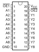 SpecificationsSupply voltage range, VCC. . . . . . . . . . . . . . . . . . . . . . . . . . . . . . . . . . . . . . . . . . . . . . . . . . . . . . . . . . 0.5 V to 7 V
Input voltage range, VI (see Note 1) . . . . . . . . . . . . . . . . . . . . . . . . . . . . . . . . . . . . . . . . . . . . . . . . . 0.5 V to 7 V
Output voltage range applied in the high or low state, VO(see Notes 1 and 2) . . . . . .. .. .. 0.5 V to VCC + 0.5 V
Output voltage range applied in high-impedance or power-off state, VO (see Note 1) . . . . . . . . .. .. 0.5 V to 7 V
Input clamp current, I IK (VI < 0) . . . . . . . . . . . . . . . . . . . . . . . . . . . . . . . . . . . . . . . . . . . . . . . . . . . . . . . . . 20 mA
Output clamp current, IOK (VO < 0 or VO > VCC ) . . . . . . . . . . . . . . . . . . . . . . . . . . . . . . . . . . . . . . . . . . . .±50 mA
Continuous output current, IO (VO = 0 to VCC ) . . . . . . . . . . . . . . . . . . . . . . . . . . . . . . . . . . . . . . . . . . . . .± 35 mA
Continuous current through VCC or GND . . . . . . . . . . . . . . . . . . . . . . . . . . . . . . . . . . . . . . . . . . . . . . . . . . . ±70 mA
Package thermal impedance, JA (see Note 3): DB package . . . . . . . . . . . . . . . . . . . . . . . . . . . . . . . . . . .. . 115/W
DGV package . . .. .. .. .. .. .. .. .. .. .. .. .. .. .. .. .. .. .. .. .. .. .. 146/W
DW package . . . . . . . . . . . . . . . . . . . . . . . . . . . . . . . . .. .. .. 97/W
NS package . . . . . . . . . . . . . . . . . . . . . . . . . . . . . . . . . . .. .. 100/W
PW package . . . . . . . . . . . . . . . . . . . . . . . . . . . . . . . . . .. .. 128/W
Storage temperature range, Tstg . . . . . . . . . . . . . . . . . . . . . . . . . . . . . . . . . . . . . . . . . . . . . . . . . . . . .65 to 150
DescriptionThe SN74LV540A devices are octal buffers/drivers designed for 2-V to 5.5-V VCC operation. These devices are ideal for driving bus lines or buffer memory address registers. They feature inputs and outputs on opposite sides of the package to facilitate printed circuit board layout.
The SN74LV540A 3-state control gate is a two-input AND gate with active-low inputs so that if either output-enable (OE1 or OE2) input is high, all corresponding outputs are in the high-impedance state. The outputs provide inverted data when they are not in the high-impedance state.
To ensure the high-impedance state during power up or power down, OE should be tied to VCC through a pullup resistor; the minimum value of the resistor is determined by the current-sinking capability of the driver.The SN54LV540A is characterized for operation over the full military temperature range of 55°C to 125°C The SN74LV540A is characterized for operation from 40°C to 85°C.

 SN74LV540A Data Sheet


