Polarity
: Non-Inverting
Maximum Operating Temperature
: + 85 C
Mounting Style
: SMD/SMT
Packaging
: Reel
Supply Voltage - Min
: 2 V
Number of Input Lines
: 8
Supply Voltage - Max
: 5.5 V
Number of Output Lines
: 3
Package / Case
: QFN-20
Features: · 2-V to 5.5-V VCC Operation
· Max tpd of 6 ns at 5 V
· Typical VOLP (Output Ground Bounce)<0.8 V at VCC = 3.3 V, TA = 25°C
· Typical VOHV (Output VOH Undershoot)>2.3 V at VCC = 3.3 V, TA = 25°C
· Support Mixed-Mode Voltage Operation on All Ports
· Ioff Supports Partial-Power-Down Mode Operation
· Latch-Up Performance Exceeds 250 mA Per JESD 17
· ESD Protection Exceeds JESD 22
− 2000-V Human-Body Model (A114-A)
− 200-V Machine Model (A115-A)
− 1000-V Charged-Device Model (C101)Pinout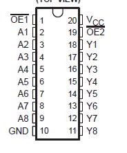 Specifications
Supply voltage range, VCC .....................................−0.5 V to 7 V
Input voltage range, VI (see Note 1) ....................−0.5 V to 7 V
Voltage range applied to any output in the high-impedance
or power-off state, VO (see Note 1)....................... −0.5 V to 7 V
Output voltage range applied in the high or low state, VO (see Notes 1 and 2) ....−0.5 V to VCC + 0.5 V
Input clamp current, IIK (VI < 0) ................................... −20 mA
Output clamp current, IOK (VO < 0) .............................. −50 mA
Continuous output current, IO (VO = 0 to VCC)............. ±35 mA
Continuous current through VCC or GND .........................±70 mA
Package thermal impedance, JA (see Note 3): DB package .......70°C/W
(see Note 3): DGV package ......92°C/W
(see Note 3): DW package........ 58°C/W
(see Note 3): NS package ......... 60°C/W
(see Note 3): PW package ..........83°C/W
(see Note 4): RGY package ...........37°C/W
Storage temperature range, Tstg .................................... −65°C to 150°C
† Stresses beyond those listed under "absolute maximum ratings" may cause permanent damage to the device. These are stress ratings only, and functional operation of the device at these or any other conditions beyond those indicated under "recommended operating conditions" is not implied. Exposure to absolute-maximum-rated conditions for extended periods may affect device reliability.
NOTES: 1. The input and output negative-voltage ratings may be exceeded if the input and output current ratings are observed.
2. This value is limited to 5.5 V maximum.
3. The package thermal impedance is calculated in accordance with JESD 51-7.
4. The package thermal impedance is calculated in accordance with JESD 51-5.
DescriptionThese devices SN74LV541ARGYR are ideal for driving bus lines or buffer memory address registers. They feature inputs and outputs on opposite sides of the package to facilitate printed circuit board layout.
The SN74LV541ARGYR 3-state control gate is a two-input AND gate with active-low inputs so that if either output-enable (OE1 or OE2) input is high, all corresponding outputs are in the high-impedance state. The outputs provide noninverted data when they are not in the high-impedance state.
To ensure the high-impedance state during power up or power down, SN74LV541ARGYR OEshould be tied to VCC through a pullup
resistor; the minimum value of the resistor is determined by the current-sinking capability of the driver.
These devices SN74LV541ARGYR are fully specified for partial-power-down applications using Ioff. The Ioff circuitry disables the outputs, preventing damaging current backflow through the devices when they are powered down.
Parameters: | Technical/Catalog Information | SN74LV541ARGYR |
| Vendor | Texas Instruments (VA) |
| Category | Integrated Circuits (ICs) |
| Logic Type | Line Driver, Non-Inverting |
| Package / Case | 20-QFN |
| Packaging | Digi-Reel? |
| Mounting Type | Surface Mount |
| Number of Bits per Element | 8 |
| Number of Elements | 1 - Single |
| Operating Temperature | -40°C ~ 85°C |
| Voltage - Supply | 2 V ~ 5.5 V |
| Current - Output High, Low | 16mA, 16mA |
| Drawing Number | 296; 4203539-4; RGY; 20 |
| Lead Free Status | Contains Lead |
| RoHS Status | RoHS Non-Compliant |
| Other Names | SN74LV541ARGYR
SN74LV541ARGYR
296 13949 6 ND
296139496ND
296-13949-6
|

 SN74LV541ARGYR Data Sheet


