SN74LVC08

Features: EPICTM (Enhanced-Performance Implanted CMOS) Submicron ProcessESD Protection Exceeds 2000 V Per Mil-STD-883C, Method 3015; Exceeds 200 V Using Machine Model (C = 200 pF, R = 0)Latch-Up Performance Exceeds 250 mA Per JEDEC Standard JESD-17Typical VOLP (Output Ground Bounce) < 0.8 V at ...

product image

SN74LVC08 Picture
SeekIC No. : 004499208 Detail

SN74LVC08: Features: EPICTM (Enhanced-Performance Implanted CMOS) Submicron ProcessESD Protection Exceeds 2000 V Per Mil-STD-883C, Method 3015; Exceeds 200 V Using Machine Model (C = 200 pF, R = 0)Latch-Up Per...

floor Price/Ceiling Price

Part Number:
SN74LVC08
Supply Ability:
5000

Price Break

  • Qty
  • 1~5000
  • Unit Price
  • Negotiable
  • Processing time
  • 15 Days
Total Cost: $ 0.00

SeekIC Buyer Protection PLUS - newly updated for 2013!

  • Escrow Protection.
  • Guaranteed refunds.
  • Secure payments.
  • Learn more >>

Month Sales

268 Transactions

Rating

evaluate  (4.8 stars)

Upload time: 2025/12/24

Payment Methods

All payment methods are secure and covered by SeekIC Buyer Protection PLUS.

Notice: When you place an order, your payment is made to SeekIC and not to your seller. SeekIC only pays the seller after confirming you have received your order. We will also never share your payment details with your seller.
Product Details

Description


Features:

 EPICTM (Enhanced-Performance Implanted CMOS) Submicron Process
 ESD Protection Exceeds 2000 V Per Mil-STD-883C, Method 3015; Exceeds 200 V Using Machine Model (C = 200 pF, R = 0)
 Latch-Up Performance Exceeds 250 mA Per JEDEC Standard JESD-17
 Typical VOLP (Output Ground Bounce) < 0.8 V at VCC = 3.3 V, TA = 25°C
Typical VOHV (Output VOH Undershoot) > 2 V at VCC = 3.3 V, TA = 25°C
 Inputs Accept Voltages to 5.5 V
 Package Options Include Plastic Small-Outline (D), Shrink Small-Outline (DB), and Thin Shrink Small-Outline (PW) Packages


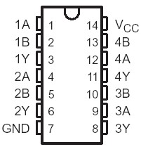
Pinout

  Connection Diagram


Specifications

Supply voltage range, VCC . . . . . . . . . . . . . . . . . . . . . . . . . . . . . . . . . . . . . . . . . . . . .0.5 V to 4.6 V
Input voltage range, VI (see Note 1) . . . . . . . . . . . .. . . .  . . . . .. . . . . . . . . . . 0.5 V to VCC + 0.5 V
Output voltage range, VO (see Notes 1 and 2) . . . . . . . . . . . . . . . . . . . . .  . . .0.5 V to VCC + 0.5 V
Input clamp current, IIK (VI < 0). . . . . . . . . . . . . . . . . . . . . . . . . . . . . . . . . . . . . . . . . . .. . . . 50 mA
Output clamp current, IOK (VO < 0 or VO > VCC) . . . . . . . . . . . . . . . . . . . . . . . . . . . . . . . . . . ±50 mA
Continuous output current, IO (VO = 0 to VCC) . . . . . . . . . . . . . . . . . . . . . . . . . . . . .. . . . . . .±50 mA
Continuous current through VCC or GND  . . . . . . . . . . . . . . . . . . . . . . . . . . . . . . . . . . . . . ... ±100mA
Maximum power package dissipation at TA = 55°C (in still air)(see Note 3):D package  . .  .. . 1.25 W
                                                                                                                     DB or PW package .0.5 W

Storage temperature range ,Tstg . . .  . . . . . . . . . . . . . . . . . . . . . . . . . . . . . . . .  .  . .65°C to 150°C 


Description

This quadruple 2-input positive-AND gate SN74LVC08 is designed for 2.7-V to 3.6-V VCC operation.

The SN74LVC08 performs the Boolean functions Y = A • B or Y = AB in positive logic.

SN74LVC08 Inputs can be driven from either 3.3-V or 5-V devices. This feature allows the use of these devices as translators in a mixed 3.3-/5-V system environment.

The SN74LVC08 is characterized for operation from 40°C to 85°C.


Customers Who Bought This Item Also Bought

Margin,quality,low-cost products with low minimum orders. Secure your online payments with SeekIC Buyer Protection.
Industrial Controls, Meters
Soldering, Desoldering, Rework Products
Line Protection, Backups
Resistors
View more