Features: EPICE (Enhanced-Performance Implanted CMOS) Submicron Process
ESD Protection Exceeds 2000 V Per MIL-STD-883, Method 3015; Exceeds 200 V Using Machine Model (C = 200 pF, R = 0)
Latch-Up Performance Exceeds 250 mA Per JESD 17
Typical VOLP (Output Ground Bounce)
< 0.8 V at VCC = 3.3 V, TA = 25°C
Typical VOHV (Output VOH Undershoot)
> 2 V at VCC = 3.3 V, TA = 25°C
Inputs Accept Voltages to 5.5 V
Package Options Include Plastic Small-Outline (D), Shrink Small-Outline (DB), and Thin Shrink Small-Outline (PW)Packages
Pinout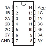 Specifications
Supply voltage range, VCC . . . . . . . . . . . . . . . . ......... . . . . . 0.5 V to 6.5 V
Input voltage range, VI (see Note 1) . . . . . .. . . .. . . . ....... . 0.5 V to 6.5 V
Output voltage range, VO (see Notes 1 and 2) ........ 0.5 V to VCC + 0.5 V
Input clamp current, IIK (VI < 0) .. . . . . . . . . . . . . . . . . . . . . . . . . . . 50 mA
Output clamp current, IOK (VO < 0) . . . . . . . . . . . . . . . . . . . . . . . . . 50 mA
Continuous output current, IO . . . . . . . . . . . . . . . . . . . ... . . . . . . . . ±50 mA
Continuous current through VCC or GND . . ........... . . . . . . . . . . . . ±100 mA
Package thermal impedance, qJA (see Note 3): D package . . . .. . 127°C/W
DB package . . . . . 158°C/W
PW package . . . . . 170°C/W
Storage temperature range, Tstg . . . . . . . . ................... . . 65°C to 150°C
‡ Stresses beyond those listed under "absolute maximum ratings" may cause permanent damage to the device. These are stress ratings only, and functional operation of the device at these or any other conditions beyond those indicated under "recommended operating conditions" is not implied. Exposure to absolute-maximum-rated conditions for extended periods may affect device reliability.
NOTES: 1. The input negative-voltage and output voltage ratings may be exceeded if the input and output current ratings are observed.
2. The value of VCC is provided in the recommended operating conditions table.
3. The package thermal impedance is calculated in accordance with JESD 51.
DescriptionThis triple 3-input positive-NAND gate SN74LVC10A is designed for 1.65-V to 3.6-V VCC operation.
The SN74LVC10A performs the Boolean function Y = A • B • C or Y = A + B + C in positive logic.
SN74LVC10A Inputs can be driven from either 3.3-V or 5-V devices. This feature allows the use of these devices as translators in a mixed 3.3-V/5-V system environment.
The SN74LVC10A is characterized for operation from 40°C to 85°C.

 SN74LVC10A Data Sheet


