Features: Member of the Texas Instruments Widebus(TM) Family
EPIC (TM) (Enhanced-Performance Implanted CMOS) Submicron Process
Typical VOLP (Output Ground Bounce) < 0.8 V at VCC = 3.3 V, TA = 25° C
Typical VOHV (Output VOH Undershoot) > 2 V at VCC = 3.3 V, TA = 25 ° C
Latch-Up Performance Exceeds 250 mA Per JEDEC Standard JESD-17
Bus Hold on Data Inputs Eliminates the Need for External Pullup/Pulldown Resistors
Package Options Include Plastic 300-mil Shrink Small-Outline (DL) and Thin Shrink Small-Outline (DGG) PackagesPinout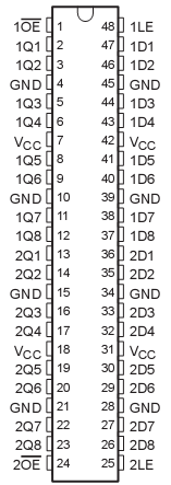 SpecificationsSupply voltage range, VCC . . . . . . . . . . . . . . . . . . . . . . 0.5 V to 4.6 V
Input voltage range, VI (see Note 1) . . . . . . . . . . . . . . 0.5 V to 4.6 V
Output voltage range, VO (see Notes 1 and 2) . 0.5 V to VCC + 0.5 V
Input clamp current, ICC (VI < 0) . . . . . . . . . . . . . . . . . . . ... . 50 mA
Output clamp current, II (VO < 0O or VCC > VCC ) . . . . . . . .. . 50 mA
Continuous output current, I (V = 0 to V ) . . . . . . .. . . . . . . . . . ±50 mA
Continuous current through VCC or GND . . . . . . .. . . . . . . ... ±100 mA
Maximum power dissipation at TA = 55°C
(in still air) (see Note 3): DGG package . . . . . . . . . .. . . . . . . . . . . 0.85 W
DL package . . . . . . . . . . . . . . . . . . . . . .. . . . . . . . .. . . . . . ... . . . . . 1.2 W
Storage temperature range, T 65° . . . . . . .. . . . . . . . . . C to 150° C
DescriptionThis 16-bit transparent D-type latch SN74LVC16373 is designed V
CC18 31 V
CC for 2.7-V
CC to 3.6-V V
CC operation.
The SN74LVC16373 is particularly suitable for 2Q6 2D6 21 28 implementing buffer registers, I/O ports, GND GND 22 27 bidirectional bus drivers, and working registers. It 2Q7 2D7 23 26 can be used as two 8-bit latches or one 16-bit 2Q8 2D8 24 25 latch. When the latch-enable (LE) input is high, the 2OE 2LE Q outputs follow the data (D) inputs. When LE is taken low, the Q outputs are latched at the levels
set up at the D inputs.
A buffered output-enable (OE) input can be used to place the eight outputs in either a normal logic state (high or low logic levels) or a high-impedance state. In the high-impedance state, the outputs neither load nor drive the bus lines significantly. The high-impedance state and the increased drive provide the capability to drive bus lines without need for interface or pullup components.
SN74LVC16373 OE does not affect internal operations of the latch. Old data can be retained or new data can be entered while the outputs are in the high-impedance state.
To ensure the high-impedance state during power up or power down, SN74LVC16373 OE should be tied to V
CC through a pullup resistor; the minimum value of the resistor is determined by the current-sinking capability of the driver.
Active bus-hold circuitry is provided to hold unused or floating data inputs at a valid logic level. The SN74LVC16373 is characterized for operation from 40°C to 85°C.

 SN74LVC16373 Data Sheet


