Features: · Member of the Texas Instruments WidebusTM Family
· EPIC E (Enhanced-Performance Implanted CMOS) Submicron Process
· Typical VOLP (Output Ground Bounce) < 0.8 V at VCC = 3.3 V, TA = 25°C
· Typical VOHV (Output VOH Undershoot) > 2 V at VCC = 3.3 V, TA = 25°C
· Latch-Up Performance Exceeds 250 mA Per JEDEC Standard JESD-17
· Bus Hold on Data Inputs Eliminates the Need for External Pullup/Pulldown Resistors
· Package Options Include Plastic 300-mil Shrink Small-Outline (DL) and Thin Shrink Small-Outline (DGG) PackagesPinout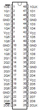 Specifications
Supply voltage range, VCC . . . . . . . . . . . . . . . . . . . . . . . . . . . . . . . . . . . . . . . .. . . . . 0.5 V to 4.6 V
Input voltage range, VI (see Note 1) . . . . . . . . . . . . . . . . . . . . . . . . . . . .. . . . . . . . . 0.5 V to 4.6 V
Output voltage range, VO (see Notes 1 and 2) . . . . . . . . . . . . . . . . . . . . . . . 0.5 V to VCC + 0.5 V
Input clamp current, IIK (VI < 0) . . . . . . . . . . . . . . . . . . . . . . . . . . . . . . . . . . . . . . . . . . . . . 50 mA
Output clamp current, IOK (VO < 0 or VO > VCC) . . . . . . . . . . . . . . . . . . . . . . . . . . . . . . . .. . ±50 mA
Continuous output current, IO (VO = 0 to VCC) . . . . . . . . . . . . . . . . . . . . . . . . . . . . . . . . . . ±50 mA
Continuous current through VCC or GND . . . . . . . . . . . . . . . . . . . . . . . . . . . . . . . . . . . .. . . ±100 mA
Maximum power dissipation at TA = 55°C (in still air) (see Note 3): DGG package . . . . . . . . 0.85 W
DL package . . . . . .. . . . . 1.2 W
Storage temperature range, Tstg . . . . . . . . . . . . . . . . . . . . . . . . . . . . . . . . . . . . . 65°C to 150°C
† Stresses beyond those listed under "absolute maximum ratings" may cause permanent damage to the device. These are stress ratings only, and functional operation of the device at these or any other conditions beyond those indicated under "recommended operating conditions" is not implied. Exposure to absolute-maximum-rated conditions for extended periods may affect device reliability.
NOTES: 1. The input and output negative-voltage ratings may be exceeded if the input and output clamp-current ratings are observed.
2. This value is limited to 4.6 V maximum.
3. The maximum package power dissipation is calculated using a junction temperature of 150°C and a board trace length of 750 mils. For more information, refer to the Package Thermal Considerations application note in the 1994 ABT Advanced BiCMOS Technology Data Book, literature number SCBD002B.
DescriptionThis 16-bit edge-triggered D-type flip-flop SN74LVC16374 is designed for 2.7-V to 3.6-V VCC operation.
The SN74LVC16374 is particularly suitable for implementing buffer registers, I/O ports, bidirectional bus drivers, and working registers. It can be used as two 8-bit flip-flops or one 16-bit flip-flop. On the positive transition of the clock (CLK) input, the Q outputs of the flip-flop take on the logic levels set up at the data (D) inputs.
A buffered output-enable (OE) input can be used to place the eight outputs in either a normal logic state (high or low logic levels) or a high-impedance state. In the high-impedance state, the outputs neither load nor drive the bus lines significantly. The high-impedance state and the increased drive provide the capability to drive bus lines without need for interface or pullup components.
SN74LVC16374 OE does not affect internal operations of the flip-flop. Old data can be retained or new data can be entered while the outputs are in the high-impedance state.
To ensure the high-impedance state during power up or power down, OE should be tied to VCC through a pullup resistor; the minimum value of the resistor is determined by the current-sinking capability of the driver.
Active bus-hold circuitry is provided to hold unused or floating data inputs at a valid logic level.
The SN74LVC16374 is characterized for operation from 40°C to 85°C.

 SN74LVC16374 Data Sheet


