Features: · Member of the Texas Instruments WidebusTM Family
· Typical VOLP (Output Ground Bounce) <0.8 V at VCC = 3.3 V, TA = 25°C
· Typical VOHV (Output VOH Undershoot) >2 V at VCC = 3.3 V, TA = 25°C
· Ioff Supports Partial-Power-Down Mode Operation
· Supports Mixed-Mode Signal Operation on All Ports (5-V Input and Output Voltages With 3.3-V VCC)
· Latch-Up Performance Exceeds 250 mA Per JESD 17
· ESD Protection Exceeds JESD 22
− 2000-V Human-Body Model (A114-A)
− 1000-V Charged-Device Model (C101)Pinout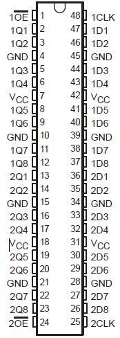 Specifications
Supply voltage range, VCC . . . . . . . . . . . . . . . . . . . . . . . . . . . .. . . . . . . . . . . . . . . . . . −0.5 V to 6.5 V
Input voltage range, VI (see Note 1) . . . . . . . . . . . . . . . . . . . . . . . . . . . . . . . . . . . . . . −0.5 V to 6.5 V
Voltage range applied to any output in the high-impedance or power-off state, VO
(see Note 1) . . . . . . . . . . . . . . . . . . . . . . . . . . . . . . . . . . . . . . . . . . . . . . . . . . . . . . . −0.5 V to 6.5 V
Voltage range applied to any output in the high or low state, VO
(see Notes 1 and 2) . . . . . . . . . . . . . . . . . . . . . . . . . . . . . . . . . . . . . . . . . . . . −0.5 V to VCC + 0.5 V
Input clamp current, IIK (VI < 0) . . . . . . . . . . . . . . . . . . . . . . . . . . . . . . . . . . . . . . . . . . . . . . . . −50 mA
Output clamp current, IOK (VO < 0) . . . . . . . . . . . . . . . . . . . . . . . . . . . . . . . . . . . . . . . . . . . . . . −50 mA
Continuous output current, IO . . . . . . . . . . . . . . . . . . . . . . . . . . . . . . . . . . . . . . . . . . . . . . . . . ±50 mA
Continuous current through each VCC or GND . . . . . . . . . . . . . . . . . . . . . . . . . . .. . . . . . . . . . ±100 mA
Package thermal impedance, JA (see Note 3): DGG package . . . . . . . . . . . . . . . . . . . . . . . . . 70°C/W
DGV package . . . . . . . . . . . . . . . . . . . . . . . . . 58°C/W
DL package . . . . . . . . . . . . . . . . . . . . . . . . . . . 63°C/W
GQL/ZQL package . . . . . . . . . . . . . . . . . . . . . . 42°C/W
Storage temperature range, Tstg . . . . . . . . . . . . . . . . . . . . . . . . . . . . . . . . . . . . . . . . −65°C to 150°C
† Stresses beyond those listed under "absolute maximum ratings" may cause permanent damage to the device. These are stress ratings only, and functional operation of the device at these or any other conditions beyond those indicated under "recommended operating conditions" is not implied. Exposure to absolute-maximum-rated conditions for extended periods may affect device reliability.
NOTES: 1. The input negative-voltage and output voltage ratings may be exceeded if the input and output current ratings are observed.
2. The value of VCC is provided in the recommended operating conditions table.
3. The package thermal impedance is calculated in accordance with JESD 51-7.
DescriptionThis 16-bit edge-triggered D-type flip-flop is designed for 1.65-V to 3.6-V VCC operation. The SN74LVC16374A is particularly suitable for implementing buffer registers, I/O ports, bidirectional bus drivers, and working registers.
The device SN74LVC16374A can be used as two 8-bit flip-flops or one 16-bit flip-flop. On the positive transition of the clock (CLK) input, the Q outputs of the flip-flop
take on the logic levels set up at the data (D) inputs.
A buffered output-enable (OE) input can be used to place the eight outputs in either a normal logic state (high or low logic levels) or the high-impedance state. In the high-impedance state, the outputs neither load nor drive the bus lines significantly. The high-impedance state and increased drive provide the capability to drive bus lines without interface or pullup components.

 SN74LVC16374A Data Sheet


