SN74LVC16646A

Features: ` Member of the Texas Instruments Widebus™ Family` Operates From 1.65 V to 3.6 V` Inputs Accept Voltages to 5.5 V` In Transparent Mode, Max tpd of 5.2 ns at 3.3 V` Typical VOLP (Output Ground Bounce) < 0.8 V at VCC = 3.3 V, TA = 25°C` Typical VOHV (Output VOH Undershoot) > 2 ...

product image

SN74LVC16646A Picture
SeekIC No. : 004499236 Detail

SN74LVC16646A: Features: ` Member of the Texas Instruments Widebus™ Family` Operates From 1.65 V to 3.6 V` Inputs Accept Voltages to 5.5 V` In Transparent Mode, Max tpd of 5.2 ns at 3.3 V` Typical VOLP (Outp...

floor Price/Ceiling Price

Part Number:
SN74LVC16646A
Supply Ability:
5000

Price Break

  • Qty
  • 1~5000
  • Unit Price
  • Negotiable
  • Processing time
  • 15 Days
Total Cost: $ 0.00

SeekIC Buyer Protection PLUS - newly updated for 2013!

  • Escrow Protection.
  • Guaranteed refunds.
  • Secure payments.
  • Learn more >>

Month Sales

268 Transactions

Rating

evaluate  (4.8 stars)

Upload time: 2025/12/24

Payment Methods

All payment methods are secure and covered by SeekIC Buyer Protection PLUS.

Notice: When you place an order, your payment is made to SeekIC and not to your seller. SeekIC only pays the seller after confirming you have received your order. We will also never share your payment details with your seller.
Product Details

Description


Features:

` Member of the Texas Instruments Widebus™ Family
` Operates From 1.65 V to 3.6 V
` Inputs Accept Voltages to 5.5 V
` In Transparent Mode, Max tpd of 5.2 ns at 3.3 V
` Typical VOLP (Output Ground Bounce) < 0.8 V at VCC = 3.3 V, TA = 25°C
` Typical VOHV (Output VOH Undershoot) > 2 V at VCC = 3.3 V, TA = 25°C
` Supports Mixed-Mode Signal Operation on All Ports (5-V Input/Output Voltage With 3.3-V VCC)
` Ioff Supports Partial-Power-Down Mode Operation
` Latch-Up Performance Exceeds 250 mA Per JESD 17
` ESD Protection Exceeds JESD 22
  2000-V Human-Body Model (A114-A)
  1000-V Charged-Device Model (C101)


Application

Audio
Automotive
Broadband
Digital Control
Military
Optical Networking
Security
Telephony
Video & Imaging
Wireless


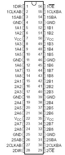
Pinout

  Connection Diagram


Specifications

MIN MAX UNIT
VCC Supply voltage range 0.5 6.5 V
VI Input voltage range(2) 0.5 6.5 V
VO Voltage range applied to any output in the high-impedance or power-off state(2) 0.5 6.5 V
VO Voltage range applied to any output in the high or low state(2) (3) 0.5 VCC + 0.5 V
IIK Input clamp current VI < 0 50 mA
IOK Output clamp current VO < 0 50 mA
IO Continuous output current ±50 mA
Continuous current through each VCC or GND ±100 mA
JA Package thermal impedance(4) DGG package 64 °C/W
DGV package 48
DL package 56
Tstg Storage temperature range 65 150 °C


Description

This 16-bit bus transceiver and register SN74LVC16646A is designed for 1.65-V to 3.6-V VCC operation.

The SN74LVC16646A can be used as two 8-bit transceivers or one 16-bit transceiver. The device consists of bus transceiver circuits, D-type flip-flops, and control circuitry arranged for multiplexed transmission of data directly from the input bus or from the internal registers.

SN74LVC16646A Data on the A or B bus is clocked into the registers on the low-to-high transition of the appropriate clock (CLKAB or CLKBA) input. Figure 1 illustrates the four fundamental bus-management functions that can be performed with the SN74LVC16646A.

SN74LVC16646A Output-enable (OE) and direction-control (DIR) inputs control the transceiver functions. In the transceiver mode, data present at the high-impedance port can be stored in either register or in both. The select-control (SAB and SBA) inputs can multiplex stored and real-time (transparent mode) data. The circuitry used for select control eliminates the typical decoding glitch that occurs in a multiplexer during the transition between stored and real-time data. DIR determines which bus receives data when OE is low. In the isolation mode (OE high), A data can be stored in one register and/or B data can be stored in the other register.

This device SN74LVC16646A is fully specified for partial-power-down applications using Ioff. The Ioff circuitry disables the outputs, preventing damaging current backflow through the device when it is powered down.

When an output function SN74LVC16646A is disabled, the input function still is enabled and can be used to store and transmit data. Only one of the two buses, A or B, can be driven at a time.

SN74LVC16646A Inputs can be driven from either 3.3-V or 5-V devices. This feature allows the use of these devices as translators in a mixed 3.3-V/5-V system environment.

To ensure the high-impedance state during power up or power down, SN74LVC16646A OE should be tied to VCC through a pullup resistor; the minimum value of the resistor is determined by the current-sinking capability of the driver.


Customers Who Bought This Item Also Bought

Margin,quality,low-cost products with low minimum orders. Secure your online payments with SeekIC Buyer Protection.