Pinout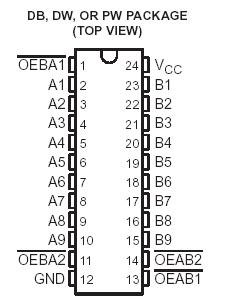 SpecificationsSupply voltage range, VCC . . . . . . . . . . . . . . . . . . . . . . . . . . . . . . . . . . . . . . . . . . . . . . . . . . . . .0.5 V to 6.5 V
Input voltage range, VI: (see Note 1) . . . . . . . . . . . . . . . . . . . . . . . . . . . . . . . . . . . . . . . . . . . . .0.5 V to 6.5 V
Voltage range applied to any output in the high-impedance or power-off state, VO
(see Note 1) . . . . . . . . . . . . . . . . . . . . . . . . . . . . . . . . . . . . . . . . . . . . . . . . . . . . . . . . . . . . . . . .0.5 V to 6.5 V
Voltage range applied to any output in the high or low state, VO
(see Notes 1 and 2) . . . . . . . . . . . . . . . . . . . . . . . . . . . . . . . . . . . . . . . . . . . . . . . . . . . . .0.5 V to VCC + 0.5 V
Input clamp current, IIK (VI < 0) . . . . . . . . . . . . . . . . . . . . . . . . . . . . . . . . . . . . . . . . . . . . . . . . . . . . . . .50 mA
Output clamp current, IOK (VO < 0) . . . . . . . . . . . . . . . . . . . . . . . . . . . . . . . . . . . . . . . . . . . . . . . . . . . . 50 mA
Continuous output current, IO . . . . . . . . . . . . . . . . . . . . . . . . . . . . . . . . . . . . . . . . . . . . . . . . . . . . . . . . ±50 mA
Continuous current through VCC or GND . . . . . . . . . . . . . . . . . . . . . . . . . . . . . . . . . . . . . . . . . . . . . . . ±100 mA
Package thermal impedance, qJA (see Note 3): DB package . . . . . . . . . . . . . . . . . . . . . . . . . . . . . . . . 104°C/W
DW package . . . . . . . . . . . . . . . . . . . . . . . . . . . . . . . . . 81°C/W
PW package . . . . . . . . . . . . . . . . . . . . . . . . . . . . . . . . 120°C/W
Storage temperature range, Tstg . . . . . . . . . . . . . . . . . . . . . . . . . . . . . . . . . . . . . . . . . . . . . . . 65°C to 150°CDescriptionThis 9-bit bus transceiver SN74LVC863A is designed for 1.65-V to 3.6-V VCC operation.
The SN74LVC863A is designed for asynchronous communication between data buses. The control-functio implementation allows for maximum flexibility in timing.
This device SN74LVC863A allows data transmission from the A bus to the B bus or from the B bus to the A bus, depending on the logic levels at the output-enable (OEAB and OEBA) inputs.
The outputs SN74LVC863A are in the high-impedance state during power-up and power-down conditions. The outputs remain in the high-impedance state while the device is powered down.
SN74LVC863A Inputs can be driven from either 3.3-V or 5-V devices. This feature allows the use of these devices as translators in a mixed 3.3-V/5-V system environment.
To ensure the high-impedance state during power up or power down, SN74LVC863A OE should be tied to VCC through a pullup resistor; the minimum value of the resistor is determined by the current-sinking capability of the driver.
The SN74LVC863A is characterized for operation from 40°C to 85°C.

 SN74LVC863A Data Sheet


