Features: Member of the Texas Instruments WidebusTM Family
EPICTM (Enhanced-Performance ImplantedCMOS) Submicron Process
Typical V OLP (Output Ground Bounce)< 0.8 V at V = 3.3 V, T = 25 CC A
Typical V OHV (Output VOH Undershoot)> 2 V at V = 3.3 V, T = 25 CC A
Power Off Disables Outputs, Permitting Live Insertion
ESD Protection Exceeds 2000 V Per MIL-STD-883, Method 3015; Exceeds 200 V Using Machine Model (C = 200 pF, R = 0)
Latch-Up Performance Exceeds 250 mA Per JESD 17
Bus Hold on Data Inputs Eliminates the Need for External Pullup/Pulldown Resistors
Supports Mixed-Mode Signal Operation on All Ports (5-V Input/Output Voltage With 3.3-V V ) CC Package Options Include Plastic 300-mil Shrink Small-Outline (DL) and Thin Shrink
Small-Outline (DGG) Packages
Pinout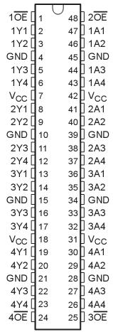 Specifications
Supply voltage range, VCC . . . . . . . . . . . . . . . . . . . . . . . . . . . . . . . . . . . . . . . . . . . . . . . . . . . . . . 0.5 V to 6.5 V
Input voltage range, VI (see Note 1) . . . . . . . . . . . . . . . . . . . . . . . . . . . . . . . . . . . . . . . . . . . . . . .0.5 V to 6.5 V
Voltage range applied to any output in the high-impedance or power-off state, VO (see Note 1) .0.5 V to 6.5 V
Voltage range applied to any output in the high or low state, VO (see Notes 1 and 2) . . . .0.5 V to VCC + 0.5 V
Input clamp current, IIK (VI < 0) . . . . . . . . . . . . . . . . . . . . . . . . . . . . . . . . . . . . . . . . . . . . . . . . . . . . . . . 50 mA
Output clamp current, IOK (VO < 0) . . . . . . . . . . . . . . . . . . . . . . . . . . . . . . . . . . . . . . . . . . . . . . . . . . . . . 50 mA
Continuous output current, IO . . . . . . . . . . . . . . . . . . . . . . . . . . . . . . . . . . . . . . . . . . . . . . . . . . . . . . . .. . ±50 mA
Continuous current through each VCC or GND . . . . . . . . . . . . . . . . . . . . . . . . . . . . . . . . . . . . . . . . . . . . ±100 mA
Package thermal impedance, JA (see Note 3): DGG package . . . . . . . . . . . . . . . . . . . . . . . . . . . . . . . . . 89/W
DL package . . . . . . . . . . . . . . . . . . . . . . . . . . . . . . . . . . . . . . . . . . . . . . . . . . . . . . . . . . . . . . . . . . . . . . . 94/W
Storage temperature range, Tstg . . . . . . . . . . . . . . . . . . . . . . . . . . . . . . . . . . . . . . . . . . . . . . . . .65 to 150
DescriptionThis 16-bit buffer/driver is designed for 1.65-V to 3.6-V VCC operation.The SN74LVCH16240A is designed specifically to improve both the performance and density of 3-state memory address drivers, clock drivers, and bus-oriented receivers and transmitters.
The device SN74LVCH16240A can be used as four 4-bit buffers, two 8-bit buffers, or one 16-bit buffer. This device provides inverting outputs and symmetrical active-low output-enable (OE) inputs.To ensure the high-impedance state during power up or power down, OE should be tied to VCC through a pullup resistor; the minimum value of the resistor is determined by the current-sinking capability of the driver. Inputs can be driven from either 3.3-V or 5-V devices. This feature allows the use of these devices as translators in a mixed 3.3-V/5-V system environment.Active bus-hold circuitry is provided to hold unused or floating data inputs at a valid logic level.
The SN74LVCH16240A is characterized for operation from 40°C to 85°C.

 SN74LVCH16240A Data Sheet


