Features: · Member of the Texas Instruments Widebus+TM Family
· EPIC E (Enhanced-Performance Implanted CMOS) Submicron Process
· UBT E (Universal Bus Transceiver) Combines D-Type Latches and D-Type Flip-Flops for Operation in Transparent, Latched, or Clocked Mode
· Typical VOLP (Output Ground Bounce) < 0.8 V at VCC = 3.3 V, TA = 25°C
· Typical VOHV (Output VOH Undershoot) > 2 V at VCC = 3.3 V, TA = 25°C
· Simultaneously Generates and Checks Parity
· Option to Select Generate Parity and Check or Feed-Through Data/Parity in A-to-B or B-to-A Directions
· Supports Mixed-Mode Signal Operation on All Ports (5-V Input/Output Voltage With 3.3-V VCC)
· Ioff Supports Partial-Power-Down-Mode Operation
· ESD Protection Exceeds 2000 V Per MIL-STD-883, Method 3015; Exceeds 200 V Using Machine Model (C = 200 pF, R = 0)
· Latch-Up Performance Exceeds 100 mA Per JESD 78, Class I
· Bus Hold on Data Inputs Eliminates the Need for External Pullup/Pulldown Resistors
· Packaged in Thin Shrink Small-Outline PackagePinout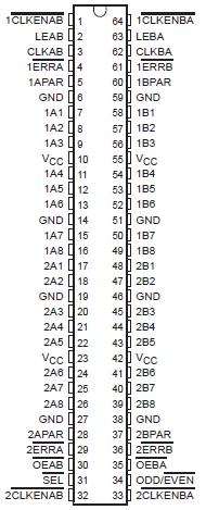 Specifications
Supply voltage range, VCC . . . . . . . . . . . . . . . . . . . . . . . . . . . . . . . . . . . . . 0.5 V to 6.5 V
Input voltage range, VI (see Note 1) . . . . . . . . . . . . . . . . . . . . . . . . . . . . . 0.5 V to 6.5 V
Voltage range applied to any output in the high-impedance or power-off state, VO
(see Note 1) . . . . . . . . . . . . . . . . . . . . . . . . . . . . . . . . . . . . . . . . . . . . . 0.5 V to 6.5 V
Voltage range applied to any output in the high or low state, VO
(see Notes 1 and 2) . . . . . . . . . . . . . . . . . . . . . . . . . . . . . . . . . . 0.5 V to VCC + 0.5 V
Input clamp current, IIK (VI < 0) . . . . . . . . . . . . . . . . . . . . . . . . . . . . . . . . . . . . . . 50 mA
Output clamp current, IOK (VO < 0) . . . . . . . . . . . . . . . . . . . . . . . . . . . . . . . . . . . . 50 mA
Continuous output current, IO . . . . . . . . . . . . . . . . . . . . . . . . . . . . . . .. . . . . . . . . ±50 mA
Continuous current through each VCC or GND . . . . . . . . . . . . . . . . . . . . . . . . . . .±100 mA
Package thermal impedance, JA (see Note 3) . . . . . . . . . . . . . . . . . . . . . . . . .. . 73°C/W
Storage temperature range, Tstg . . . . . . . . . . . . . . . . . . . . . . . . . . . .. . .65°C to 150°C
† Stresses beyond those listed under "absolute maximum ratings" may cause permanent damage to the device. These are stress ratings only, and functional operation of the device at these or any other conditions beyond those indicated under "recommended operating conditions" is not implied. Exposure to absolute-maximum-rated conditions for extended periods may affect device reliability.
NOTES: 1. The input negative-voltage and output voltage ratings may be exceeded if the input and output current ratings are observed.
2. The value of VCC is provided in the recommended operating conditions table.
3. The package thermal impedance is calculated in accordance with JESD 51.
DescriptionThis 18-bit (dual-octal) noninverting registered transceiver SN74LVCH16901 is designed for 1.65-V to 3.6-V VCC operation.
The SN74LVCH16901 is a dual 9-bit to dual 9-bit parity transceiver with registers. The device can operate as a feed-through transceiver, or it can generate/check parity from the two 8-bit data buses in either direction.
The SN74LVCH16901 features independent clock (CLKAB or CLKBA), latch-enable (LEAB or LEBA), and dual 9-bit clock-enable (CLKENAB or CLKENBA) inputs. It also provides parity-enable (SEL) and parity-select (ODD/EVEN) inputs and separate error-signal (ERRA or ERRB) outputs for checking parity. The direction of data flow is controlled by output-enable (OEAB and OEBA) inputs. When SEL is low, the parity functions are enabled. When SEL is high, the parity functions are disabled, and the device acts as an 18-bit registered transceiver.

 SN74LVCH16901 Data Sheet


