SN74LVCR16245A

Features: *Member of the Texas Instruments WidebusTM Family* Operates From 1.65 V to 3.6 V* Inputs Accept Voltages to 5.5 V* Max tpd of 4.8 ns at 3.3 V* Typical VOLP (Output Ground Bounce) <0.8 V at VCC = 3.3 V, TA = 25* Typical VOHV (Output VOH Undershoot) >2 V at VCC = 3.3 V, TA = 25* Supp...

product image

SN74LVCR16245A Picture
SeekIC No. : 004499408 Detail

SN74LVCR16245A: Features: *Member of the Texas Instruments WidebusTM Family* Operates From 1.65 V to 3.6 V* Inputs Accept Voltages to 5.5 V* Max tpd of 4.8 ns at 3.3 V* Typical VOLP (Output Ground Bounce) <0.8 V...

floor Price/Ceiling Price

Part Number:
SN74LVCR16245A
Supply Ability:
5000

Price Break

  • Qty
  • 1~5000
  • Unit Price
  • Negotiable
  • Processing time
  • 15 Days
Total Cost: $ 0.00

SeekIC Buyer Protection PLUS - newly updated for 2013!

  • Escrow Protection.
  • Guaranteed refunds.
  • Secure payments.
  • Learn more >>

Month Sales

268 Transactions

Rating

evaluate  (4.8 stars)

Upload time: 2025/12/24

Payment Methods

All payment methods are secure and covered by SeekIC Buyer Protection PLUS.

Notice: When you place an order, your payment is made to SeekIC and not to your seller. SeekIC only pays the seller after confirming you have received your order. We will also never share your payment details with your seller.
Product Details

Description


Features:

* Member of the Texas Instruments
   WidebusTM Family
* Operates From 1.65 V to 3.6 V
* Inputs Accept Voltages to 5.5 V
* Max tpd of 4.8 ns at 3.3 V
* Typical VOLP (Output Ground Bounce)
   <0.8 V at VCC = 3.3 V, TA = 25
* Typical VOHV (Output VOH Undershoot)
   >2 V at VCC = 3.3 V, TA = 25
* Supports Mixed-Mode Signal Operation on
   All Ports (5-V Input/Output Voltage With
   3.3-V VCC)
* All Inputs and Outputs Have Equivalent
   26-Ω Series Resistors, So No External
   Resistors Are Required
* Ioff Supports Partial-Power-Down Mode
   Operation
* Latch-Up Performance Exceeds 250 mA Per
   JESD 17
* ESD Protection Exceeds JESD 22
   − 2000-V Human-Body Model (A114-A)
   − 200-V Machine Model (A115-A)


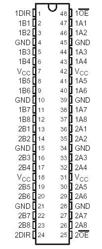
Pinout

  Connection Diagram


Specifications

Supply voltage range, VCC  . . . . . . . . . . . . . . . . . . . . . . . . . . . . . . . . . . . . . . . . . . . . . . . . .−0.5 V to 6.5 V
Input voltage range, VI (see Note 1)  . . . . . . . . . . . . . . . . . . . . . . . . . . . . . . . . . . . . . . . . .−0.5 V to 6.5 V
Voltage range applied to any output in the high-impedance or power-off state, VO
(see Note 1)  . . . . . . . . . . . . . . . . . . . . . . . . . . . . . . . . . . . . . . . . . . . . . . . . . . . . . . . . . . . .−0.5 V to 6.5 V
Voltage range applied to any output in the high or low state, VO
(see Notes 1 and 2) . . . . . . . . . . . . . . . . . . . . . . . . . . . . . . . . . . . . . . . . . . . . .... . . .−0.5 V to VCC + 0.5 V
Input clamp current, IIK (VI < 0) . . . . . . . . . . . . . . . . . . . . . . . . . . . . . . . . . . . . . . . . . . . . . . . . . . .−50 mA
Output clamp current, IOK (VO < 0) . . . . . . . . . . . . . . . . . . . . . . . . . . . . . . . . . . . . . . . . . . . . . . . . .−50 mA
Continuous output current, IO  . . . . . . . . . . . . . . . . . . . . . . . . . . . . . . . . . . . . . . . . . . ... . . . . . . . .±50 mA
Continuous current through each VCC or GND . . . . . . . . . . . . . . . . . . . . . . . . . . . . . . . . .  . . . . . .±100 mA
Package thermal impedance, JA (see Note 3): DGG package  . . . . . . . . . . . . . . . . . . . . . . .  . . . . .70/W
                                                                          DGV package  . . . . . . . . . . . . . . . . . . . . . . . . . . . . .58/W
                                                                          DL package  . . . . . . . . . . . . . . . . . . . . . . . .   . . . . .63/W
                                                                          GQL/ZQL package  . . . . . . . . . . . . . . . . . . . .. . . . . .42/W
Storage temperature range, Tstg  . . . . . . . . . . . . . . . . . . . . . . . . . . . . . . . . . . . . . . . .. . . . .−65 to 150


Description

This 16-bit (dual-octal) noninverting bus transceiver SN74LVCR16245A is designed for 1.65-V to 3.6-V VCC operation.

The SN74LVCR16245A is designed for asynchronous communication between data buses. The control-function implementation minimizes external-timing requirements.

This device SN74LVCR16245A can be used as two 8-bit transceivers or one 16-bit transceiver. It allows data transmission from the A bus to the B bus or from the B bus to the A bus, depending on the logic level at the direction-control (DIR) input. The output-enable (OE) input can disable the device so that the buses are effectively isolated.

SN74LVCR16245A All outputs, which are designed to sink up to 12 mA, include equivalent 26- series resistors to reduce overshoot and undershoot.

SN74LVCR16245A Inputs can be driven from either 3.3-V or 5-V devices. This feature allows the use of this device as a translator in a mixed 3.3-V/5-V system environment.

To ensure the high-impedance state during power up or power down, SN74LVCR16245A OE should be tied to VCC through a pullup resistor; the minimum value of the resistor is determined by the current-sinking capability of the driver.

This device SN74LVCR16245A is fully specified for partial-power-down applications using Ioff. The Ioff circuitry disables the outputs, preventing damaging current backflow through the device when it is powered down.


Customers Who Bought This Item Also Bought

Margin,quality,low-cost products with low minimum orders. Secure your online payments with SeekIC Buyer Protection.
LED Products
Line Protection, Backups
Prototyping Products
DE1
Tapes, Adhesives
803
Fans, Thermal Management
Crystals and Oscillators
View more