ApplicationAudio
Automotive
Broadband
Digital Control
Military
Optical Networking
Security
Telephony
Video & Imaging
WirelessPinout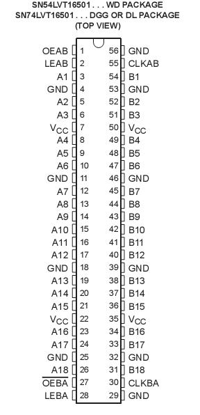 Specifications
Supply voltage range, VCC . . . . . . . . . . . . . . . . . . . . . . . . . . . . . . . . . . . . . . . . . . . . . . . . . . 0.5 V to 4.6 V
Input voltage range, VI (see Note 1) . . . . . . . . . . . . . . . . . . . . . . . . . . . . . . . . . . . . . . . . . . . 0.5 V to 7 V
Voltage range applied to any output in the high state or power-off state, VO (see Note 1) . .0.5 V to 7 V
Current into any output in the low state, IO : SN54LVT16501 . . . . . . . . . . . . . . . . . . . . . . . . . . . . . . . 96 mA
SN74LVT16501 . . . . . . . . . . . . . . . . . . . . . . . . . . . . ... 128 mA
Current into any output in the high state, IO (see Note 2): SN54LVT16501 . . . . . . . . . . . . . . . . . . .. . 48 mA
SN74LVT16501 . . . . . . . . . . . . . . . . . . . ...64 mA.
Input clamp current, IIK (VI < 0) . . . . . . . . . . . . . . . . . . . . . . . . . . . . . . . . . . . . . . . . . . . . . . . . . . . . 50 mA
Output clamp current, IOK (VO < 0) . . . . . . . . . . . . . . . . . . . . . . . . . . . . . . . . . . . . . . . . . . . . . . . . . 50 mA
Maximum power dissipation at TA = 55 (in still air) (see Note 3):DGG package . . . . . . . . . . . . . . . . ..... 1 W
DL package . . . . . . . . . . . . . . . ...... 1.4 W
Storage temperature range, Tstg . . . . . . . . . . . . . . . . . . . . . . . . . . . . . . . . . . . . . . . . . . . . . . .65 to 150
DescriptionThe SN74LVT16501 are 18-bit universal bus transceivers designed for low-voltage (3.3-V) V CC operation, but with the capability to provide a TTL interface to a 5-V system environment.
Data flow in each direction is controlled by output-enable (OEAB and OEBA), latch-enable (LEAB and LEBA), and clock (CLKAB and CLKBA) inputs. For A-to-B data flow, the devices SN74LVT16501 operate in the transparent mode when LEAB is high. When LEAB is low, the A data is latched if CLKAB is held at a high or low logic level. If LEAB is low, the A-bus data is stored in the latch/flip-flop on the low-to-high transition of CLKAB. When OEAB is high, the outputs are active. When OEAB is low, the outputs are in the high-impedance state.
Data flow for B to A is similar to that of A to B but uses OEBA, OEBA, and CLKBA. The output enables are complementary (OEAB is active high and OEBA is active low).
Active bus-hold circuitry SN74LVT16501 is provided to hold unused or floating data inputs at a valid logic level.
About SN74LVT16501, To ensure the high-impedance state during power up or power down, OEshould be tied to VCC through a pullup resistor. The minimum value of the resistor is determined by the current-sinking capability of the driver. OE should be tied to GND through a pulldown resistor; the minimum value of the resistor is determined by the current-sourcing capability of the driver.
The SN74LVT16501 is available in TI's shrink small-outline (DL) and thin shrink small-outline (DGG) packages, which provide twice the input/output (I/O) pin count and functionality of standard small-outline packages in the same printed circuit board area.
The SN54LVT16501 is characterized for operation over the full military temperature range of 55 to 125. The SN74LVT16501 is characterized for operation from 40 to 85.

 SN74LVT16501 Data Sheet


