SN74LVT244

Features: • State-of-the-Art Advanced BiCMOS Technology (ABT) Design for 3.3-V Operation and Low Static Power Dissipation• Support Mixed-Mode Signal Operation (5-V Input and Output Voltages With 3.3-V VCC)• Support Unregulated Battery Operation Down to 2.7 V• Typical VOLP (...

product image

SN74LVT244 Picture
SeekIC No. : 004499439 Detail

SN74LVT244: Features: • State-of-the-Art Advanced BiCMOS Technology (ABT) Design for 3.3-V Operation and Low Static Power Dissipation• Support Mixed-Mode Signal Operation (5-V Input and Output Volta...

floor Price/Ceiling Price

Part Number:
SN74LVT244
Supply Ability:
5000

Price Break

  • Qty
  • 1~5000
  • Unit Price
  • Negotiable
  • Processing time
  • 15 Days
Total Cost: $ 0.00

SeekIC Buyer Protection PLUS - newly updated for 2013!

  • Escrow Protection.
  • Guaranteed refunds.
  • Secure payments.
  • Learn more >>

Month Sales

268 Transactions

Rating

evaluate  (4.8 stars)

Upload time: 2025/12/24

Payment Methods

All payment methods are secure and covered by SeekIC Buyer Protection PLUS.

Notice: When you place an order, your payment is made to SeekIC and not to your seller. SeekIC only pays the seller after confirming you have received your order. We will also never share your payment details with your seller.
Product Details

Description


Features:

• State-of-the-Art Advanced BiCMOS Technology (ABT) Design for 3.3-V Operation and Low Static Power Dissipation
• Support Mixed-Mode Signal Operation (5-V Input and Output Voltages With 3.3-V VCC)
• Support Unregulated Battery Operation Down to 2.7 V
• Typical VOLP (Output Ground Bounce) < 0.8 V at VCC = 3.3 V, TA = 25°C
• ESD Protection Exceeds 2000 V Per MIL-STD-883C, Method 3015; Exceeds 200 V Using Machine Model (C = 200 pF, R = 0)
• Latch-Up Performance Exceeds 500 mA Per JEDEC Standard JESD-17
• Bus-Hold Data Inputs Eliminate the Need for External Pullup Resistors
• Supports Live Insertion
• Package Options Include Plastic Small-Outline (DW), Shrink Small-Outline (DB), and Thin Shrink Small-Outline (PW) Packages, Ceramic Chip Carriers (FK), Ceramic Flatpacks (W), and Ceramic DIPS (J)


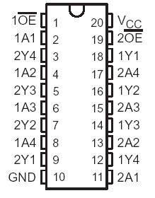
Pinout

  Connection Diagram


Specifications

Supply voltage range, VCC . . . . . . . . . . . . . . . . . . . . . . . . . . . . . . . . . . . . . . .  . . . . . . 0.5 V to4.6 V
Input voltage range, V (see Note 1) . . . . . . . . . . . . . . . . . . . . . . . . . . . .  . . . . . . . . . 0.5 V to 7 V
Voltage applied to any output in the high state or power-off state, VO (see Note 1). . 0.5 V to 7 V
Current into any output in the low state, IO: SN54LVT244 . . . . . . . . . . . .. . . . . . . . . . . . ..   . .96 mA 
                                                                       SN74LVT244 . . . . . . . . . . . . . . . . . . . . .  . . ..   .128 mA
Current into any output in the high state, IO (see Note 2): SN54LVT244 . . . . . . . . . .. . . . . . . .48 mA
                                                                                             SN74LVT244  . . . . . . . . .  . . . . .. . .64 mA

Input clamp current, IIK (VI < 0) . . . . . . . . . . . . . . . . . . . . . . . . . . . . . . . .. . . . . . . . . . . . . . .. .50 mA
Output clamp current, IOK (VO < 0)  . . . . . . . . . . . . . . . . . . . . . . . . . . . . . . . . . . . . . . . . . . . . .50 mA
Maximum power dissipation at TA = 55°C (in still air) (see Note 3): DB package  . . . .  . . . .  . . .0.6 W
                                                                                                         DW package  . . . .. . . . .  .. .1.6 W
                                                                                                         PW package  . . . . . . . . . . . .0.7 W
Storage temperature range  . . . . . . . . . . . . . . . . . . . . . . . . . . . . . . . . . . . . . . . . .. . . .65°C to 150°C


Description

These octal buffers and line drivers SN74LVT244 are designed specifically for low-voltage (3.3-V) VCC operation, but with the capability to provide a TTL interface to a 5-V system environment.

The SN74LVT244 is organized as two 4-bit line drivers with separate output-enable (OE) inputs. When OE is low, the device passes data from the A inputs to the Y outputs. When OE is high, the outputs are in the high-impedance state.

Active bus-hold circuitry is provided by SN74LVT244 to hold unused or floating data inputs at a valid logic level.

About SN74LVT244,To ensure the high-impedance state during power up or power down, OE should be tied to VCC through a pullup resistor; the minimum value of the resistor is determined by the current-sinking capability of the driver.

The SN74LVT244 is packaged in TI's shrink small-outline package (DB), which provides the same I/O pin count and functionality of standard small-outline packages in less than half the printed-circuit-board area.

The SN54LVT244 is characterized for operation over the full military temperature range of 55°C to 125°C. The SN74LVT244 is characterized for operation from 40°C to 85°C.


Customers Who Bought This Item Also Bought

Margin,quality,low-cost products with low minimum orders. Secure your online payments with SeekIC Buyer Protection.
Cables, Wires
Integrated Circuits (ICs)
Undefined Category
Circuit Protection
Tapes, Adhesives
803
View more