Features: ` Members of the Texas Instruments (TI) Family of JTAG Scan-Support Products
` Extend Scan Access From Board Level to Higher Level of System Integration
` Three IEEE Std 1149.1-Compatible Configurable Secondary Scan Paths to One Primary Scan Path
` Multiple Devices Can Be Cascaded to Link 24 Secondary Scan Paths to One Primary Scan Path
` Simple (Linking Shadow) Protocol Is Used to Connect the Primary Test Access Port (TAP) to Secondary TAPs. This Single Protocol Is Used to Address and Configure the Secondary Scan Path.
` The LASP(8986) and ASP(8996) Can Be Configured on the Same Backplane Using Similar Shadow Protocols
` Linking Shadow Protocols Can Occur in Any of Test-Logic-Reset, Run-Test/Idle, Pause-DR, Pause-IR TAP States to Provide Board-to-Board and Built-In Self-Test
` Bypass (BYP5BYP0) Forces Primary to Configured Secondary Paths Without Use of Linking Shadow Protocols
` Connect (CON2CON0) Provides Indication of Primary-to-Secondary Paths Connections
` Secondary TAPs Can Be Configured at High Impedance Via the OE Input to Allow an Alternate Test Master to Take Control of the Secondary TAPs
` High-Drive Outputs (32 mA IOH, 64 mA IOL) Support Backplane Interface at Primary Outputs and High Fanout at Secondary Outputs
` While Powered at 3.3 V, Both the Primary and Secondary TAPs Are Fully 5-V Tolerant for Interfacing 5-V and/or 3.3-V Masters and Targets
` Package Options Include Plastic BGA (GGV) and LQFP (PM) Packages and Ceramic Quad Flat (HV) Packages Using 25-mil Center-to-Center Spacing
Pinout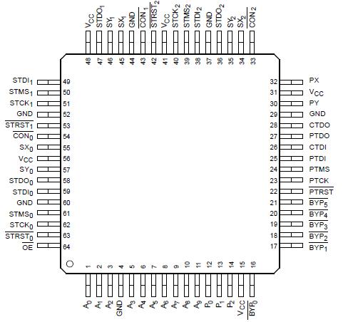 Specifications
Supply voltage range, VCC . . . . . . . . . . . . . . . . . . . . . . . . . . . . . . . . . . . . . . . . . . . . . . 0.5 V to 4.6 V
Input voltage range, VI (see Note 1) . . . . . . . . . . . . . . . . . . . . . . . . . . . . . . . . . . . . . . . 0.7 V to 7 V
Voltage range applied to any output in the high-impedance or power-off state, VO
(see Note 1) . . . . . . . . . . . . . . . . . . . . . . . . . . . . . . . . . . . . . . . . . . . . . . . . . . . . . . . . . 0.5 V to 7 V
Current into any output in the low state, IOL: SN54LVT8986 . . . . . . . . . . . . . . . . . . . . . . . . . . . 96 mA
SN74LVT8986 . . . . . . . . . . . . . . . . . . . . . . . . . 128 mA
Current into any output in the high state, IO (see Note 2): SN54LVT8986 . . . . . . . . . . . . . . . . 48 mA
SN74LVT8986 . . . . . . . . . . . . . . . . . 64 mA
Input clamp current, IIK (VI < 0) . . . . . . . . . . . . . . . . . . . . . . . . . . . . . . . . . . . . . . . . . . . . . . . . ±20 mA
Output clamp current, IOK (VO < 0) . . . . . . . . . . . . . . . . . . . . . . . . . . . . . . . . . . . . . . . . . . . . . . ±20 mA
Continuous output current, IO (VO = 0 to VCC) . . . . . . . . . . . . . . . . . . . . . . . . . . . . . . . . . . . . . ±35 mA
Storage temperature range, Tstg . . . . . . . . . . . . . . . . . . . . . . . . . . . . . . . . . . . . . . . . 65°C to 150°C
† Stresses beyond those listed under "absolute maximum ratings" may cause permanent damage to the device. These are stress ratings only, and functional operation of the device at these or any other conditions beyond those indicated under "recommended operating conditions" is not implied. Exposure to absolute-maximum-rated conditions for extended periods may affect device reliability.
NOTES: 1. The input and output negative-voltage ratings can be exceeded if the input and output clamp-current ratings are observed.
2. This current flows only when the output is in the high state and VO > VCC.
DescriptionThe SN74LVT8986 Linking Addressable Scan Ports (LASPs) are members of the Texas Instruments family of IEEE Std 1149.1 (JTAG) scan-support products. The scan-support product family facilitates testing of fully boundary-scannable devices. The LASP applies linking shadow protocols through the test access port (TAP) to extend scan access to the system level and divide scan chains at the board level.
The LASP SN74LVT8986 consists of a primary TAP for interfacing to the backplane IEEE Std 1149.1 serial-bus signals (PTDI, PTMS, PTCK, PTDO, PRTST) and three secondary TAPs for interfacing to the board-level IEEE Std 1149.1 serial-bus signals. Each secondary TAP consists of signals STDIx, STMSx, STCKx, STDOx, and STRSTX. Conceptually, the LASP is a simple switch that can be used to connect directly a set of primary TAP signals to a set of secondary TAP signals-for example, to interface backplane TAP signals to a board-level TAP. The LASP SN74LVT8986 provides all signal buffering that might be required at these two interfaces. Primary-to-secondary TAP connections can be configured with the help of linking shadow protocol or protocol bypass (BYP5BYP0) inputs. All possible configurations are tabulated in Function Tables 1, 2, and 3.

 SN74LVT8986 Data Sheet


