Features: Members of the Texas InstrumentsWidebusTM Family
State-of-the-Art Advanced BiCMOSTechnology (ABT) Design for 3.3-VOperation and Low Static-PowerDissipation
Support Mixed-Mode Signal Operation(5-V Input and Output Voltages With3.3-V VCC )
Support Unregulated Battery OperationDown to 2.7 V
Typical VOLP(Output Ground Bounce)< 0.8 V at VCC = 3.3 V, TA = 25
Ioffand Power-Up 3-State Support HotInsertion
Bus Hold on Data Inputs Eliminates theNeed for External Pullup/PulldownResistors
Distributed VCC and GND Pin ConfiguratioMinimizes High-Speed Switching Noise
Flow-Through Architecture Optimizes PCBLayout
Latch-Up Performance Exceeds 500 mA PeJESD 17
ESD Protection Exceeds 2000 V PerMIL-STD-883, Method 3015; Exceeds 200 VUsing Machine Model (C = 200 pF, R = 0)
Package Options Include Plastic Shrink
Small-Outline (DL) and Thin Shrink
Small-Outline (DGG) Packages and 380-mi
Fine-Pitch Ceramic Flat (WD) Package
Using 25-mil Center-to-Center Spacings
Pinout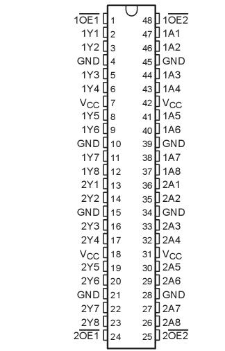 Specifications
Supply voltage range, VCC . . . . . . . . . . . . . . . . . . . . . . . . . . . . . . . . . . . . . . . . . . . . . . . 0.5 V to 4.6 V
Input voltage range, VI(see Note 1) . . . . . . . . . . . . . . . . . . . . . . . . . . . . . . . . . . . . . . . . . 0.5 V to 7 V
Voltage range applied to any output in the high-impedance
or power-off state, VO (see Note 1) . . . . . .. . . . . . . . . . . . . . . . . . . . . . . . . .. . . . . . . . . . 0.5 V to 7 V
Voltage range applied to any output in the high state, VO (see Note 1) . . . . . . .. . 0.5 V to VCC , 0.5 V
Current into any output in the low state, IO : SN54LVTH16541 . . . . . . . . . . . . . . . . . . . . . . . . . . . . 96 mA
SN74LVTH16541 . . . . . . . . . . . . . . . . . . . . .. . . . . . 128 mA
Current into any output in the high state, IO (see Note 2): SN54LVTH16541 . . . . . . . . . . . . . . . . . 48 mA
SN74LVTH16541 . . . . . . . . . . . . . . . . . . 64 mA
Input clamp current, IIK (VI < 0) . . . . . . . . . . . . . . . . . . . . . . . . . . . . . . . . . . . . . . . . . . . . . . . . . . . 50 mA
Output clamp current, IOK(VO< 0) . . . . . . . . . . . . . . . . . . . . . . . . . . . . . . . . . . . . . . . . . . . . . . . . . . 50 mA
Package thermal impedance, JA (see Note 3): DGG package . . . . . . . . . . . . . . . . . . . . . . . . . . . . . . 89/W
DL package . . . . . . . . . . . . . . . . .. . . .. . . .. . . . . . . . . . . . . . . . . . . . . . 94/W
Storage temperature range, Tstg . . . . . . . . . . . . . . . . . . . . . . . . . . . . . . . . . . . . . . . . . . . . . . 65to 150
DescriptionThese 16-bit buffers/drivers SN74LVTH16541 are designed specifically for low-voltage (3.3-V) VCCoperation, but with thecapability to provide a TTL interface to a 5-V system environment.
These devices are noninverting 16-bit buffers composed of two 8-bit sections with separate output-enablesignals. For either 8-bit buffer section, the two output-enable (1OE1 and 1OE2 or 2OE1 and 2OE2) inputs mustbe low for the corresponding Y outputs to be active. If either output-enable input is high, the outputs of that 8-bitbuffer section are in the high-impedance state.
When VCC is between 0 and 1.5 V, the devices are in the high-impedance state during power up or power down.
About SN74LVTH16541, to ensure the high-impedance state above 1.5 V, OE should be tied to VCCthrough a pullup resistor;the minimum value of the resistor is determined by the current-sinking capability of the driver.
Active bus-hold circuitry is provided to hold unused or floating data inputs at a valid logic level.
These devices SN74LVTH16541 are fully specified for hot-insertion applications using I and power-up 3-state. The I circuitryoff offdisables the outputs, preventing damaging current backflow through the devices when they are powered down.
The power-up 3-state circuitry places the outputs in the high-impedance state during power up and power down, which prevents driver conflict.
The SN54LVTH16541 is characterized for operation over the full military temperature range of 55°C to 125°C.The SN74LVTH16541 is characterized for operation from 40°C to 85°C.

 SN74LVTH16541 Data Sheet


