SN74LVTH182646A

Features: Members of the Texas Instruments SCOPE TMFamily of Testability Products Members of the Texas Instruments WidebusTMFamily State-of-the-Art 3.3-V ABT Design Supports Mixed-Mode Signal Operation (5-V Input and Output Voltages With 3.3-V VCC) Support Unregulated Battery Operation Down to 2....

product image

SN74LVTH182646A Picture
SeekIC No. : 004499479 Detail

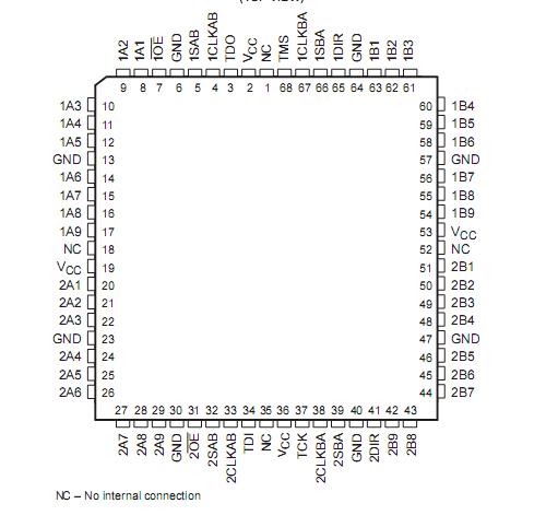
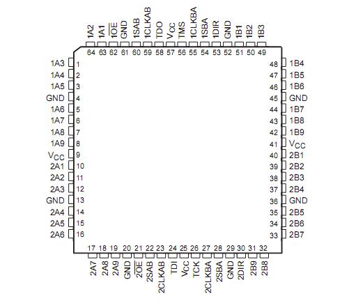
SN74LVTH182646A: Features: Members of the Texas Instruments SCOPE TMFamily of Testability Products Members of the Texas Instruments WidebusTMFamily State-of-the-Art 3.3-V ABT Design Supports Mixed-Mode Signal Opera...

floor Price/Ceiling Price

Part Number:
SN74LVTH182646A
Supply Ability:
5000

Price Break

  • Qty
  • 1~5000
  • Unit Price
  • Negotiable
  • Processing time
  • 15 Days
Total Cost: $ 0.00

SeekIC Buyer Protection PLUS - newly updated for 2013!

  • Escrow Protection.
  • Guaranteed refunds.
  • Secure payments.
  • Learn more >>

Month Sales

268 Transactions

Rating

evaluate  (4.8 stars)

Upload time: 2025/12/24

Payment Methods

All payment methods are secure and covered by SeekIC Buyer Protection PLUS.

Notice: When you place an order, your payment is made to SeekIC and not to your seller. SeekIC only pays the seller after confirming you have received your order. We will also never share your payment details with your seller.
Product Details

Description


Features:

 Members of the Texas Instruments SCOPE TMFamily of Testability Products
 Members of the Texas Instruments  WidebusTMFamily
  State-of-the-Art 3.3-V ABT Design Supports Mixed-Mode Signal Operation (5-V Input and Output Voltages With 3.3-V VCC)
  Support Unregulated Battery Operation Down to 2.7 V
  Include D-Type Flip-Flops and Control Circuitry to Provide Multiplexed Transmission of Stored and Real-Time Data
  Bus Hold on Data Inputs Eliminates the Need for External Pullup/Pulldown Resistors
  B-Port Outputs of 'LVTH182646A Devices Have Equivalent 25-Ω Series Resistors, So No External Resistors Are Required
  Compatible With IEEE Std 1149.1-1990 (JTAG) Test Access Port and Boundary-Scan Architecture
 SCOPE Instruction Set
    IEEE Std 1149.1-1990 Required Instructions and Optional CLAMP and HIGHZ
    Parallel-Signature Analysis at Inputs
    Pseudo-Random Pattern Generation
  From Outputs
    Sample Inputs/Toggle Outputs
    Binary Count From Outputs
    Device Identification
    Even-Parity Opcodes
  Packaged in 64-Pin Plastic Thin Quad Flat (PM) Packages Using 0.5-mm Center-to-Center Spacings and 68-Pin
     Ceramic Quad Flat (HV) Packages Using 25-mil Center-to-Center Spacings


Pinout

  Connection Diagram  Connection Diagram


Specifications

Supply voltage range, VCC. . . . . . . . . . . . . . . . . . . . . . . . . . . . . . . . . . . . . . . . . . . . . . . . 0.5 V to 4.6 V
Input voltage range, VI. . . . . . . . . . . . . . . . . . . . . . . . . . . . . . . . . . . . . . . . . . (see Note 1) 0.5 V to 7 V
Voltage range applied to any output in the high or power-off state, VO. . . . . (see Note 1) 0.5 V to 7 V
Current into any output in the low state, IO :SN54LVTH18646A. . . . . . . . . . . . . . . . . . . . . . . . . . . 96 mA
                                                                       SN54LVTH182646A (A port or TDO) . . . . . . . . . . . . .  96 mA
                                                                       SN54LVTH182646A (B port). . . . . . . . . . . . . . . . . . . . 30 mA
                                                                       SN74LVTH18646A . . . . . . . . . . . . . . . . . . . . . . . . .. .128 mA
                                                                       SN74LVTH182646A (A port or TDO) . . . . . . . . . . . .  128 mA
                                                                       SN74LVTH182646A (B port) . . . . . . . . . . . . . . . . . . .. 30 mA

Current into any output in the high state, IO (see Note 2):SN54LVTH18646A . . . . . . . . . . . . . . . . . 48 mA
                                                                                            SN54LVTH182646A (A port or TDO) . . . . 48 mA
                                                                                            SN54LVTH182646A (B port) . . . . . . . . . . 30 mA
                                                                                            SN74LVTH18646A . . . . . . . . . . . . . . . . . .64 mA
                                                                                            SN74LVTH182646A (A port or TDO) . . . . 64 mA
                                                                                            SN74LVTH182646A (B port) . . . . . . . . . . 30 mA
Input clamp current, IIK (VI< 0) . . . . . . . . . . . . . . . . . . . . . . . . . . . . . . . . . . . . . . . . . . . . . . . . . . . . 50 mA
Output clamp current, IOK (VO < 0) . . . . . . . . . . . . . . . . . . . . . . . . . . . . . . . . . . . . . . . . . . . . . . . . . .50 mA
Package thermal impedance, JA (see Note 3): PM package. . . . . . . . . . . . . . . . . . . . . . . . . . . . . . .67°C/W
Storage temperature range, Tstg . . . . . . . . . . . . . . . . . . . . . . . . . . . . . . . . . . . . . . . . . . . . .65°C to 150°C


†Stresses beyond those listed under "absolute maximum ratings" may cause permanent damage to the device. These are stress ratings only, and functional operation of the device at these or any other conditions beyond those indicated under "recommended operating conditions" is not implied. Exposure to absolute-maximum-rated conditions for extended periods may affect device reliability.

NOTES:
1.The input and output negative-voltage ratings can be exceeded if the input and output clamp-current ratings are observed.
2.This current flows only when the output is in the high state and V> VCC.
3.The package thermal impedance is calculated in accordance with JESD 51.


Description

The 'LVTH18646A and SN74LVTH182646A scan test devices with 18-bit bus transceivers and registers are members of the Texas Instruments (TI) SCOPE testability integrated-circuit family. This family of devices supports IEEE Std 1149.1-1990 boundary scan to facilitate testing of complex circuit board assemblies. Scan access to the test circuitry is accomplished via the 4-wire test access port (TAP) interface. Additionally, these devices SN74LVTH182646A are designed specifically for low-voltage (3.3-V) VCC operation, but with thecapability to provide a TTL interface to a 5-V system environment.

In the normal mode, these devices SN74LVTH182646A are 18-bit bus transceivers and registers that allow for multiplexed transmission of data directly from the input bus or from the internal registers. They can be used either as two 9-bit transceivers or one 18-bit transceiver. The test circuitry can be activated by the TAP to take snapshot samples of the data appearing at the device pins or to perform a self test on the boundary-test cells. Activating the TAP in the normal mode does not affect the functional operation of the SCOPE bus transceivers and registers.

Transceiver function is controlled by output-enable (OE ) and direction (DIR) inputs. When OE  is low, the transceiver is active and operates in the A-to-B direction when DIR is high or in the B-to-A direction when DIR is low. WhenOE is high, both the A and B outputs are in the high-impedance state, effectively isolating both buses.

About SN74LVTH182646A,Data flow is controlled by clock (CLKAB and CLKBA) and select (SAB and SBA) inputs. Data on the A bus is clocked into the associated registers on the low-to-high transition of CLKAB. When SAB is low, real-time A data is selected for presentation to the B bus (transparent mode). When SAB is high, stored A data is selected for presentation to the B bus (registered mode). The function of the CLKBA and SBA inputs mirrors that of CLKAB and SAB, respectively. Figure 1 shows the four fundamental bus-management functions that can be performed with the 'LVTH18646A and 'LVTH182646A.

In the test mode, the normal operation of the SCOPE bus transceivers and registers is inhibited, and the test circuitry is enabled to observe and control the I/O boundary of the device SN74LVTH182646A. When enabled, the test circuitry performs boundary-scan test operations according to the protocol described in IEEE Std 1149.1-1990. Four dedicated test pins are used to observe and control the operation of the test circuitry: test data input (TDI), test data output (TDO), test mode select (TMS), and test clock (TCK). Additionally, the test circuitry performs other testing functions such as parallel-signature analysis (PSA) on data inputs and pseudo-random pattern generation (PRPG) from data outputs. All testing and scan operations are synchronized to the TAP interface.

Active bus-hold circuitry is provided by SN74LVTH182646A to hold unused or floating data inputs at a valid logic level. The B-port outputs of 'LVTH182646A, which are designed to source or sink up to 12 mA, include equivalent 25-Ω series resistors to reduce overshoot and undershoot. The SN54LVT18646 and SN54LVTH182646A are characterized for operation over the full military temperature range of 55°C to 125°C. The SN74LVTH18646A and SN74LVTH182646A are characterized for operation from40°C to 85°C.


Customers Who Bought This Item Also Bought

Margin,quality,low-cost products with low minimum orders. Secure your online payments with SeekIC Buyer Protection.
Line Protection, Backups
Crystals and Oscillators
Power Supplies - Board Mount
Circuit Protection
View more