Features: · State-of-the-Art Advanced BiCMOS Technology (ABT) Design for 3.3-V Operation and Low Static-Power Dissipation
· Ioff and Power-Up 3-State Support Hot Insertion
· Bus Hold on Data Inputs Eliminates the Need for External Pullup/Pulldown Resistors
· Support Mixed-Mode Signal Operation (5-V Input and Output Voltages With 3.3-V VCC)
· Support Unregulated Battery Operation Down to 2.7 V
· Typical VOLP (Output Ground Bounce)< 0.8 V at VCC = 3.3 V, TA = 25°C
· Latch-Up Performance Exceeds 500 mA Per JESD 17
· ESD Protection Exceeds 2000 V Per MIL-STD-883, Method 3015; Exceeds 200 V Using Machine Model (C = 200 pF, R = 0)
· Package Options Include Plastic Small-Outline (DW), Shrink Small-Outline (DB), and Thin Shrink Small-Outline (PW) Packages, Ceramic Chip Carriers (FK), Ceramic Flat (W) Package, and Ceramic (J ) DIPs
Pinout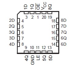
SpecificationsSupply voltage range, VCC . . . . . . . . . . . . . . . . . . . . . . . . . . .. . . . . . . . . . . . . . . . . . . . . . . . 0.5 V to 4.6 V
Input voltage range, VI (see Note 1) . . . . . . . . . . . . . . . . . . . . . . . . . . . . . . . . . . . . . . . . . . . . 0.5 V to 7 V
Voltage range applied to any output in the high-impedance
or power-off state, VO (see Note 1) . . . . . . . . . . . . . . . . . . . . . . . . . . . . . . . . . . . . . . . . . . . . . 0.5 V to 7 V
Voltage range applied to any output in the high state, VO (see Note 1) . . . . . . . . . . . 0.5 V to VCC + 0.5 V
Current into any output in the low state, IO: SN54LVTH373 . . . . . . . . . . . . . . . . . . . . . . . . . . . . . . . . 96 mA
SN74LVTH373 . . . . . . . . . . . . . . . . . . . . . . . . . . . . . . . 128 mA
Current into any output in the high state, IO (see Note 2): SN54LVTH373 . . . . . . . . . . . . . . . . . . . . . 48 mA
SN74LVTH373 . . . . . . . . . . . . . . . . . . . . . . . 64 mA
Input clamp current, IIK (VI < 0) . . . . . . . . . . . . . . . . . . . . . . . . . . . . . . . . . . . . . . . . . . . . . . . . . . . . . 50 mA
Output clamp current, IOK (VO < 0) . . . . . . . . . . . . . . . . . . . . . . . . . . . . . . . . . . . . . . . . . . . . . . . . . . . 50 mA
Package thermal impedance, qJA (see Note 3): DB package . . . . . . . . . . . . . . . . . . . . . . . . . . . . . . 115°C/W
DW package . . . . . . . . . . . . . . . . . . . . . . . . . . . . . . 97°C/W
PW package . . . . . . . . . . . . . . . . . . . . . . . .. . . . . . 128°C/W
Storage temperature range, Tstg . . . . . . . . . . . . . . . . . . . . . . . . . . . . . . . . . . . . . . . . . . .. . 65°C to 150°C
† Stresses beyond those listed under "absolute maximum ratings" may cause permanent damage to the device. These are stress ratings only, and functional operation of the device at these or any other conditions beyond those indicated under "recommended operating conditions" is not implied. Exposure to absolute-maximum-rated conditions for extended periods may affect device reliability.
NOTES: 1. The input and output negative-voltage ratings may be exceeded if the input and output clamp-current ratings are observed. 2. This current flows only when the output is in the high state and VO > VCC. 3. The package thermal impedance is calculated in accordance with JESD 51.
DescriptionThese octal latches SN74LVTH373 are designed specifically for low-voltage (3.3-V) VCC operation, but with the capability to provide a TTL interface to a 5-V system environment.
About SN74LVTH373,While the latch-enable (LE) input is high, the Q outputs follow the data (D) inputs. When LE is taken low, the Q outputs are latched at the logic levels set up at the D inputs.
About SN74LVTH373,A buffered output-enable (OE) input can be used to place the eight outputs in either a normal logic state (high or low logic levels) or a high-impedance state. In the high-impedance state, the outputs neither load nor drive the bus lines significantly. The high-impedance state and increased drive provide the capability to drive bus lines without need for interface or pullup components.
OE does not affect the internal operations of the latches. Old data can be retained or new data can be entered while the outputs are in the high-impedance state.
When VCC is between 0 and 1.5 V, the devices SN74LVTH373 are in the high-impedance state during power up or power down. owever, to ensure the high-impedance state above 1.5 V, OE should be tied to VCC through a pullup resistor; the minimum value of the resistor is determined by the current-sinking capability of the driver.
Active bus-hold circuitry is provided to hold unused or floating data inputs at a valid logic level.

 SN74LVTH373 Data Sheet


