Features: · EPIC E (Enhanced-Performance Implanted CMOS) 2-m Process
· Typical VOLP (Output Ground Bounce) < 0.8 V at VCC, TA = 25°C
· Typical VOHV (Output VOH Undershoot) > 2 V at VCC, TA = 25°C
· ESD Protection Exceeds 2000 V Per MIL-STD-883C, Method 3015; Exceeds 200 V Using Machine Model (C = 200 pF, R = 0)
· Latch-Up Performance Exceeds 250 mA Per JEDEC Standard JESD-17
· Package Options Include Plastic Small-Outline (D), Shrink Small-Outline (DB), Thin Shrink Small-Outline (PW), and Ceramic Flat (W) Packages, Ceramic Chip Carriers (FK), and Ceramic (J) 300-mil DIPs
Pinout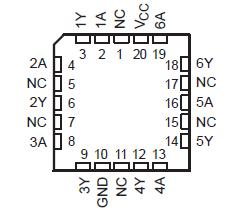 Specifications
Supply voltage range, VCC . . . . . . . . . . . . . . . . . . . . . . . . . . . . . . . . . . . . . . . . . . . . . . 0.5 V to 7 V
Input voltage range, VI (see Note 1) . . . . . . . . . . . . . . . . . . . . . . . . . . . . . . . . 0.5 V to VCC + 0.5 V
Output voltage range, VO (see Notes 1 and 2) . . . . . . . . . . . . . . . . . . . . . . . . 0.5 V to VCC + 0.5 V
Input clamp current, IIK (VI < 0 or VI > VCC) . . . . . . . . . . . . . . . . . . . . . . . . . . . . . . . . . . . . . ±20 mA
Output clamp current, IOK (VO < 0 or VO > VCC) . . . . . . . . . . . . . . . . . . . . . . . . . . . . . . . . . . ±50 mA
Continuous output current, IO (VO = 0 to VCC) . . . . . . . . . . . . . . . . . . . . . . . . . . . . . . . . . . . ±25 mA
Continuous current through VCC or GND . . . . . . . . . . . . . . . . . . . . . . . . . . . . . . . . . . . . . . . . ±50 mA
Maximum power dissipation at TA = 55°C (in still air) (see Note 3): D package . . . . . . . . . . . 1.25 W
DB or PW package . . . . . . 0.5 W
Storage temperature range, Tstg . . . . . . . . . . . . . . . . . . . . . . . . . . . . . . . . . . . . . . 65°C to 150°C
‡ Stresses beyond those listed under "absolute maximum ratings" may cause permanent damage to the device. These are stressratings only, and functional operation of the device at these or any other conditions beyond those indicated under "recommended operating conditions" is not implied. Exposure to absolute-maximum-rated conditions for extended periods may affect device reliability.
NOTES: 1. The input and output voltage ratings may be exceeded if the input and output current ratings are observed.
2. This value is limited to 7 V maximum.
3. The maximum package power dissipation is calculated using a junction temperature of 150°C and a board trace length of 750 mils.
DescriptionThese hex inverters SN74LVU04 are designed for 2.7-V to 5.5-V VCC operation.
The SN74LVU04 contain six independent inverters with unbuffered outputs. These devices perform the Boolean function Y = A.
The SN74LVU04 is available in TI's shrink small-outline package (DB), which provides the same I/O pin count and functionality of standard small-outline packages in less than half the printed-circuit-board area.
The SN54LVU04 is characterized for operation over the full military temperature range of 55°C to 125°C. The SN74LVU04 is characterized for operation from 40°C to 85°C.

 SN74LVU04 Data Sheet


