Features: ` Member of the Texas Instruments WidebusTM Family
` Supports SSTL_2 Signal Data Inputs and Outputs
` Supports LVTTL Switching Levels on the RESET Pin
` Differential CLK Signal
` Flow-Through Architecture Optimizes PCB Layout
` Meets SSTL_2 Class II Specifications
` Latch-Up Performance Exceeds 100 mA Per JESD 78, Class II
` ESD Protection Exceeds JESD 22
2000-V Human-Body Model (A114-A)
200-V Machine Model (A115-A)
1000-V Charged-Device Model (C101)
` Packaged in Plastic Thin Shrink Small-Outline PackagePinout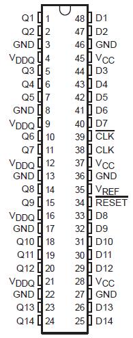 Specifications
Supply voltage range, VCC or VDDQ . . . . . . . . . . . . . . . . . . . . . . . . . . . . . . . . 0.5 V to 4.6 V
Input voltage range, VI (see Note 1) . . . . . . . . . . . . . . . . . . . . . . . .. . 0.5 V to VDDQ + 0.5 V
Output voltage range, VO (see Notes 1 and 2) . . . . . . . . . . . . . . . . . 0.5 V to VDDQ + 0.5 V
Input clamp current, IIK (VI < 0) . . . . . . . . . . . . . . . . . . . . . . . . . . . . . . . . . . . . . . . . . 50 mA
Output clamp current, IOK (VO < 0) . . . . . . . . . . . . . . . . . . . . . . . . . . . . . . . . . . . . . . . 50 mA
Continuous output current, IO (VO = 0 to VDDQ) . . . . . . . . . . . . . . . . . . . . . . . . .. . . . ±50 mA
Continuous current through each VCC, VDDQ, or GND . . . . . . . . . . . . . . . . . . . . . . . . ±100 mA
Package thermal impedance, JA (see Note 3) . . . . . . . . . . . . . . . . . . . . . . . . . . . . . . 70°C/W
Storage temperature range, Tstg . . . . . . . . . . . . . . . . . . . . . . . . . . . . . . . . . 65°C to 150°C
† Stresses beyond those listed under "absolute maximum ratings" may cause permanent damage to the device. These are stress ratings only, and functional operation of the device at these or any other conditions beyond those indicated under "recommended operating conditions" is not implied. Exposure to absolute-maximum-rated conditions for extended periods may affect device reliability.
NOTES: 1. The input and output negative-voltage ratings may be exceeded if the input and output clamp-current ratings are observed.
2. Current flows only when the output is in the high state and VO > VDDQ.
3. The package thermal impedance is calculated in accordance with JESD 51.
DescriptionThis 14-bit registered buffer SN74SSTL16857 is designed for 2.3-V to 3.6-V VCC operation and SSTL_2 data input and output levels.
About SN74SSTL16857,All inputs are compatible with the JEDEC Standard for SSTL_2, except the LVCMOS reset (RESET) input. All outputs are SSTL_2, Class II compatible.
About SN74SSTL16857,When RESET is low, the differential input receivers are disabled, and undriven (floating) data and clock inputs are allowed. In addition, when RESET is low, all registers are reset, and all outputs are forced low. The LVCMOS RESET input must always be held at a valid logic high or low level.To ensure defined outputs from the register before a stable clock has been supplied, RESET must be held in the low state during power up.
The SN74SSTL16857 is characterized for operation from 0°C to 70°C.

 SN74SSTL16857 Data Sheet


