SN74SSTU32864

Features: ` Member of the Texas Instruments Widebus+ Family` Pinout Optimizes DDR-II DIMM PCB Layout` Configurable as 25-Bit 1:1 or 14-Bit 1:2 Registered Buffer` Chip-Select Inputs Gate the Data Outputs from Changing State and Minimizes System Power Consumption` Output Edge-Control Circuit...

product image

SN74SSTU32864 Picture
SeekIC No. : 004499535 Detail

SN74SSTU32864: Features: ` Member of the Texas Instruments Widebus+ Family` Pinout Optimizes DDR-II DIMM PCB Layout` Configurable as 25-Bit 1:1 or 14-Bit 1:2 Registered Buffer` Chip-Select Inputs Gate the ...

floor Price/Ceiling Price

Part Number:
SN74SSTU32864
Supply Ability:
5000

Price Break

  • Qty
  • 1~5000
  • Unit Price
  • Negotiable
  • Processing time
  • 15 Days
Total Cost: $ 0.00

SeekIC Buyer Protection PLUS - newly updated for 2013!

  • Escrow Protection.
  • Guaranteed refunds.
  • Secure payments.
  • Learn more >>

Month Sales

268 Transactions

Rating

evaluate  (4.8 stars)

Upload time: 2025/12/24

Payment Methods

All payment methods are secure and covered by SeekIC Buyer Protection PLUS.

Notice: When you place an order, your payment is made to SeekIC and not to your seller. SeekIC only pays the seller after confirming you have received your order. We will also never share your payment details with your seller.
Product Details

Description


Features:

` Member of the Texas Instruments Widebus+ Family
` Pinout Optimizes DDR-II DIMM PCB Layout
` Configurable as 25-Bit 1:1 or 14-Bit 1:2 Registered Buffer
` Chip-Select Inputs Gate the Data Outputs from Changing State and Minimizes System Power Consumption
` Output Edge-Control Circuitry Minimizes Switching Noise in an Unterminated Line
` Supports SSTL_18 Data Inputs
` Differential Clock (CLK and CLK) Inputs
` Supports LVCMOS Switching Levels on the Control and RESET Inputs
RESET Input Disables Differential Input Receivers, Resets All Registers, and Forces All Outputs Low
` Latch-Up Performance Exceeds 100 mA Per JESD 78, Class II
` ESD Protection Exceeds JESD 22 5000-V Human-Body Model (A114-A) 200-V Machine Model (A115-A)
1000-V Charged-Device Model (C101)


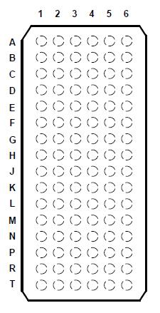
Pinout

  Connection Diagram


Specifications

Supply voltage range, VCC. . . . . . . . . . . . . . . . . . . . . . . . . . . . . . . . . . 0.5 V to 2.5 V
Input voltage range, VI (see Notes 1 and 2) .. . . . . . . . . . . . . . . . . . . 0.5 V to 2.5 V
Output voltage range, VO (see Notes 1 and 2). . . . . . . . . . . . . 0.5 V to VCC + 0.5 V
Input clamp current, IIK (VI < 0 or VI > VCC). . . . . . . . . . . . . . . . . . . . . . . . . . ±50 mA
Output clamp current, IOK (VO < 0 or VO > VCC)  . . . . . . . . . . . . . . . . . . . . . . ±50 mA
Continuous output current, IO (VO = 0 to VCC) .. . . . . . . . . . . . . . . . . . . . . . . ±50 mA
Continuous current through each VCC or GND .  . . . . . . . . . . . . . . . . . . . . . . ±100 mA
Package thermal impedance, JA (see Note 3). . .. . . . . . . . . . . . . . . . . . . . . . 36°C/W
Storage temperature range, Tstg. . . . . . . . . . . . . . . . . . . . . . . . . . . . . . 65to 150
† Stresses beyond those listed under "absolute maximum ratings" may cause permanent damage to the device. These are stress ratings only, and functional operation of the device at these or any other conditions beyond those indicated under "recommended operating conditions" is not implied. Exposure to absolute-maximum-rated conditions for extended periods may affect device reliability.
NOTES: 1. The input and output negative-voltage ratings may be exceeded if the input and output clamp-current ratings are observed.
2. This value is limited to 2.5 V maximum.
3. The package thermal impedance is calculated in accordance with JESD 51-7.


Description

This 25-bit 1:1 or 14-bit 1:2 configurable registered buffer SN74SSTU32864 is designed for 1.7-V to 1.9-V VCC operation. In the 1:1 pinout configuration, only one device per DIMM is required to drive nine SDRAM loads. In the 1:2 pinout configuration, two devices per DIMM are required to drive 18 SDRAM loads.
. SSTL_18, except the LVCMOS reset (RESET) and LVCMOS control (Cn) inputs. All outputs are edge-controlled circuits optimized for unterminated DIMM loads and meet SSTL_18 specifications.The SN74SSTU32864 operates from a differential clock (CLK andCLK). Data are registered at the crossing of CLK going high and CLK going low.

The C0 input controls the pinout configuration of the 1:2 pinout from register-A configuration (when low) to register-B configuration (when high). The C1 input controls the pinout configuration from 25-bit 1:1 (when low) to 14-bit 1:2 (when high). C0 and C1 should not be switched during normal operation. They should be hard-wired to a valid low or high level to configure the register in the desired mode. In the 25-bit 1:1 pinout configuration,the A6, D6, and H6 terminals are driven low and should not be used.

The device SN74SSTU32864 supports low-power standby operation. When RESET is low, the differential input receivers are disabled, and undriven (floating) data, clock, and reference voltage (VREF) inputs are allowed. In addition, when RESET is low, all registers are reset and all outputs are forced low. The LVCMOSRESET and Cn inputs always must be held at a valid logic high or low level.

About SN74SSTU32864,The two VREF pins (A3 and T3), are connected together internally by approximately 150 . However, it is necessary to connect only one of the two VREF pins to the external VREF power supply. An unused VREF pin should be erminated with a VREF coupling capacitor.


Customers Who Bought This Item Also Bought

Margin,quality,low-cost products with low minimum orders. Secure your online payments with SeekIC Buyer Protection.
Batteries, Chargers, Holders
Integrated Circuits (ICs)
Isolators
Discrete Semiconductor Products
Tapes, Adhesives
803
View more