Pinout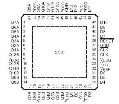 Specifications
Supply voltage range, VCC or VDDQ . . . . . . . . . . . . . . . . . . . . . . . . . . . . . . . . . .−0.5 V to 3.6 V
Input voltage range, VI (see Notes 1 and 2) . . . . . . . . . . . . . . . . . . . . . .−0.5 V to VCC + 0.5 V
Output voltage range, VO (see Notes 1 and 2) . . . . . . . . . . . . . . . . . .−0.5 V to VDDQ + 0.5 V
Input clamp current, IIK (VI < 0) . . . . . . . . . . . . . . . . . . . . . . . . . . . . . . . . . . . . . . . . . .−50 mA
Output clamp current, IOK (VO < 0 or VO > VDDQ) . . . . . . . . . . . . . . . . . . . . . . . . . . . . .±50 mA
Continuous output current, IO (VO = 0 to VDDQ) . . . . . . . . . . . . . . . . . . . . . . . . . . . . .±50 mA
Continuous current through each VCC, VDDQ, or GND . . . . . . . . . . . . . . . . . .. . . . . . .±100 mA
Package thermal impedance, JA (see Note 3): DGG package . . . . . . . . . . . . . . . . . . .55°C/W
(see Note 4): RGQ package . . . . . . . . . . . . . . . . . .22°C/W
Storage temperature range, Tstg . . . . . . . . . . . . . . . . . . . . . . . . . . . . . . . . . .−65°C to 150°C
DescriptionThis 13-bit to 26-bit registered buffer SN74SSTV16859 is designed for 2.3-V to 2.7-V VCC operation.All inputs are SSTL_2, except the LVCMOS reset (RESET) input. All outputs are SSTL_2, Class II compatible.
The SN74SSTV16859 operates from a differential clock (CLK and CLK).Data are registered at the crossing of CLK going high and CLK going low.
The device SN74SSTV16859 supports low-power standby operation. When RESET is low, the differential input receivers are disabled, and undriven (floating) data, clock, and reference voltage (VREF) inputs are allowed. In addition, when RESET is low, all registers are reset, and all outputs are forced low. The LVCMOS RESET input always must be held at a valid logic high or low level.To ensure defined outputs from the register before a stable clock has been supplied,RESET must be held in the low state during power up.

 SN74SSTV16859 Data Sheet


