SN74TVC16222A

Features: Member of the Texas Instruments Widebus FamilyDesigned to Be Used in Voltage-Limiting Applications6.5- On-State Connection Between Ports A and BFlow-Through Pinout for Ease of Printed Circuit Board Trace RoutingDirect Interface With GTL+ LevelsESD Protection Exceeds JESD 22 ͨ...

product image

SN74TVC16222A Picture
SeekIC No. : 004499546 Detail

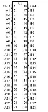
SN74TVC16222A: Features: Member of the Texas Instruments Widebus FamilyDesigned to Be Used in Voltage-Limiting Applications6.5- On-State Connection Between Ports A and BFlow-Through Pinout for Ease of Prin...

floor Price/Ceiling Price

Part Number:
SN74TVC16222A
Supply Ability:
5000

Price Break

  • Qty
  • 1~5000
  • Unit Price
  • Negotiable
  • Processing time
  • 15 Days
Total Cost: $ 0.00

SeekIC Buyer Protection PLUS - newly updated for 2013!

  • Escrow Protection.
  • Guaranteed refunds.
  • Secure payments.
  • Learn more >>

Month Sales

268 Transactions

Rating

evaluate  (4.8 stars)

Upload time: 2025/12/24

Payment Methods

All payment methods are secure and covered by SeekIC Buyer Protection PLUS.

Notice: When you place an order, your payment is made to SeekIC and not to your seller. SeekIC only pays the seller after confirming you have received your order. We will also never share your payment details with your seller.
Product Details

Description


Features:

 Member of the Texas Instruments Widebus Family
 Designed to Be Used in Voltage-Limiting Applications
 6.5- On-State Connection Between Ports A and B
 Flow-Through Pinout for Ease of Printed Circuit Board Trace Routing
 Direct Interface With GTL+ Levels
 ESD Protection Exceeds JESD 22
    − 2000-V Human-Body Model (A114-A)
    − 200-V Machine Model (A115-A)
    − 1000-V Charged-Device Model (C101)


Pinout

  Connection Diagram


Specifications

Input voltage range, VI (see Note 1) . . . . . . . . . . . . . . . . . . . . . . . . . . . . . . . . . . . . . . . . . . . . . . −0.5 V to 7 V
Input/output voltage range, VI/O (see Note 1) . . . . . . . . . . . . . . . . . . . . . . . . . . . . . . . . . . . .. . . −0.5 V to 7 V
Continuous channel current . . . . . . . . . . . . . . . . . . . . . . . . . . . . . . . . . . . . . . . . . . . . . . . . . . . . . . . . . . 128 mA
Input clamp current, IIK (VI < 0) . . . . . . . . . . . . . . . . . . . . . . . . . . . . . . . . . . . . . . . . . . . . . . . . . . . . . .. −50 mA
Package thermal impedance, JA (see Note 2): DGG package . . . . . . . . . . . . . . . . . . . . . . . . . . . . . . . 70°C/W
                                                                           DGV package . . . . . . . . . . . . . . . . . . . . . . . . . . . . . .   58°C/W
                                                                           DL package . . . . . . . . . . . . . . . . . . . . . . . . . . . . . . . .. 63°C/W
Storage temperature range, Tstg . . . . . . . . . . . . . . . . . . . . . . . . . . . . . . . . . . . . . . . . . . . . . . −65°C to 150°C
NOTES: 1. The input and input/output negative-voltage ratings may be exceeded if the input and input/output clamp-current ratings are observed.
             2. The package thermal impedance is calculated in accordance with JESD 51-7.


Description

The SN74TVC16222A provides 23 parallel NMOS pass transistors with a common gate. The low on-state resistance of the switch allows connections to be made with minimal propagation delay.

The device SN74TVC16222A can be used as a 22-bit switch, with the gates cascaded together to a reference transistor.The low-voltage side of each pass transistor is limited to a voltage set by the reference transistor. This is done to protect components with inputs that are sensitive to high-state voltage-level overshoots. (See Application Information in this data sheet.)

All of the SN74TVC16222A transistors in the TVC array have the same electrical characteristics; therefore, any one of them can be used as the reference transistor. Because, within the device, the characteristics from transistor to transistor are equal, the maximum output high-state voltage (VOH) is approximately the reference voltage (VREF), with minimal deviation from one output to another. This is a benefit of the TVC solution over discrete devices. Because the fabrication of the transistors is symmetrical, either port connection of each bit can be used as the low-voltage side, and the I/O signals are bidirectional through each FET.


Customers Who Bought This Item Also Bought

Margin,quality,low-cost products with low minimum orders. Secure your online payments with SeekIC Buyer Protection.
Motors, Solenoids, Driver Boards/Modules
Optoelectronics
Cable Assemblies
RF and RFID
Fans, Thermal Management
View more